

Image sensor and formation method thereof
An image sensor and substrate technology, applied in radiation control devices and other directions, can solve the problems affecting the imaging quality of the image sensor and the reduction of quantum efficiency, and achieve the effects of reducing longitudinal leakage current, improving light absorption rate, and improving consistency
- Summary
- Abstract
- Description
- Claims
- Application Information
AI Technical Summary
Problems solved by technology
Method used
Image

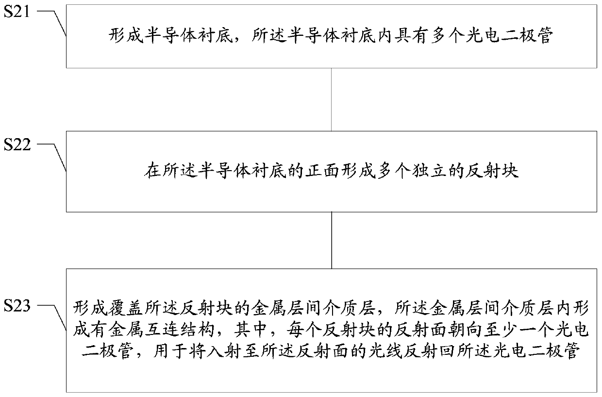
Examples
Embodiment Construction
[0027] In existing image sensors, part of the light will pass through the photodiode without being absorbed, resulting in a decrease in quantum efficiency and affecting the imaging quality of the image sensor.
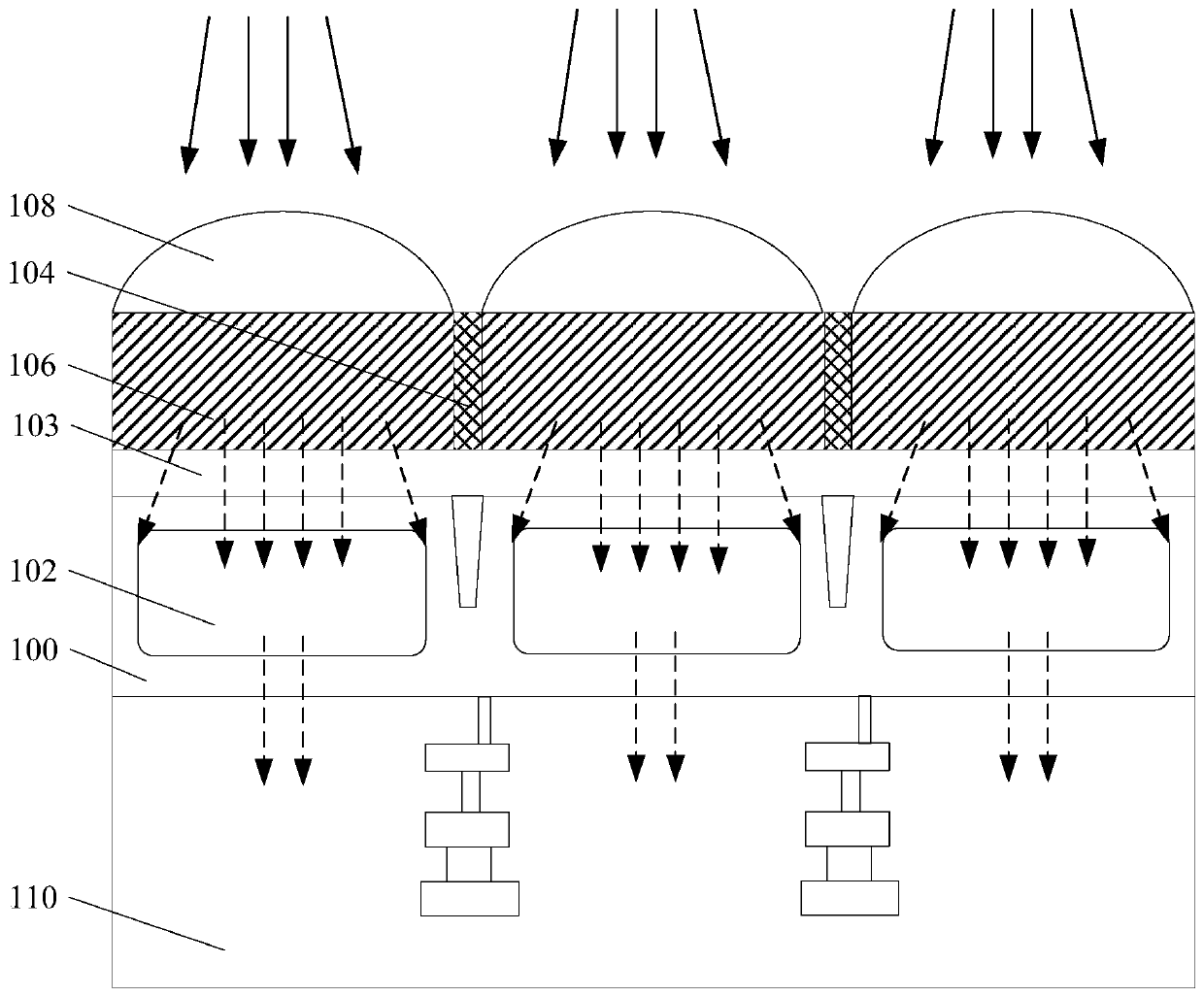
[0028] refer to figure 1 , figure 1 It is a schematic cross-sectional structure diagram of an image sensor in the prior art.
[0029] In an existing image sensor, a semiconductor substrate 100 can be provided, metal grids 104 are formed on the surface of the semiconductor substrate 100, and filter structures 106 are formed in the openings between the metal grids 104, and then filter structures 106 are formed in the openings between the metal grids 104. The surface of the mirror structure 106 forms a lens structure 108 .
[0030] Wherein, a logic device, a pixel device and a metal interconnection layer are formed in the semiconductor substrate 100, the pixel device may include a photodiode 102, and the metal interconnection layer may include a metal interconnection st...
PUM
 Abstract
Description
Claims
Application Information