A multimode multi-frequency radio frequency power amplifier

A radio frequency power, multi-mode and multi-frequency technology, which is applied in power amplifiers, high-frequency amplifiers, amplifier input/output impedance improvements, etc., can solve the problems of unadjustable first section, need to improve integration, and difficult to design bandwidth, etc. , to achieve the effect of reducing the number and occupying the substrate area, improving the harmonic suppression effect, and simplifying the chip packaging process

Pending Publication Date: 2019-05-21
RDA MICROELECTRONICS TECH SHANGHAI CO LTD
View PDF5 Cites 20 Cited by
  • Summary
  • Abstract
  • Description
  • Claims
  • Application Information

AI Technical Summary

Problems solved by technology

Third, the power of the GSM low frequency band is twice the power of the GSM high frequency band. For example, sharing a bare chip amplification channel, how to improve the efficiency of the GSM high frequency band under the premise of meeting the performance of the GSM low frequency band is also a difficult problem
Fifth, the frequency span from the GSM low frequency band to the Band41 frequency band of the TDD-LTE network standard is very large, and it is difficult to design such a wide bandwidth with a matching circuit
The scheme is a single-input-multiple-output structure as a whole, and the degree of integration still needs to be improved; the shared first segment cannot be adjusted, which reduces the adjustability
In addition, the efficiency, harmonic suppression capability, linearity, and bandwidth range of the RF power amplifier are all important performance indicators, and this scheme does not involve

Method used


Image

  • A multimode multi-frequency radio frequency power amplifier
  • A multimode multi-frequency radio frequency power amplifier
  • A multimode multi-frequency radio frequency power amplifier

Examples


Embodiment Construction

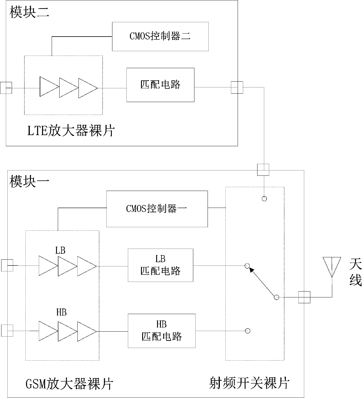
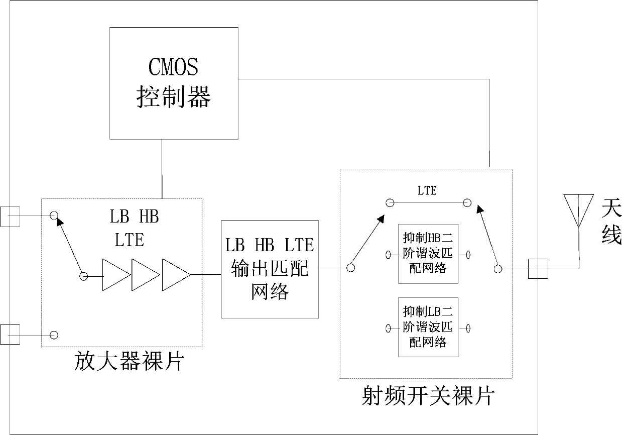
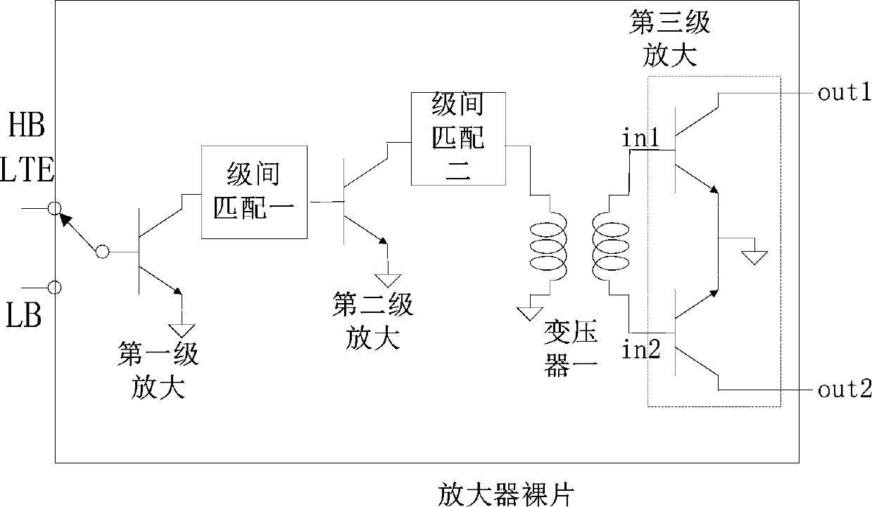
[0030] see figure 2 , which is the multi-mode multi-frequency radio frequency power amplifier of the present application. It is only a module, for example a substrate. This module is also responsible for voice communication and data communication, including amplifier die, radio frequency switch die and some peripheral devices. The amplifier bare chip has only one amplification path, and simultaneously realizes amplification for signals of the GSM low frequency band, the GSM high frequency band and the LTE frequency band. The amplifying path has two input terminals and one output terminal, the first input terminal is a signal of GSM high frequency band or LTE frequency band, the second input terminal is a signal of GSM low frequency band, and the output terminal is connected to an output matching network. The radio frequency switch bare chip includes three paths, and the signal output from the matching network is connected to one of the paths and then connected to the antenn...


PUM


Abstract

The invention discloses a multimode multi-frequency radio frequency power amplifier. The multimode multi-frequency radio frequency power amplifier comprises an amplifier bare chip, an output matchingnetwork, a radio frequency switch bare chip and a CMOS controller. The amplifier bare chip is provided with only one amplification path, and amplification of signals of all frequency bands is achievedat the same time. The output matching network is arranged between the amplifier bare chip and the radio frequency switch bare chip and is used for carrying out impedance matching on each frequency band signal. The radio frequency switch bare chip comprises three paths, and a signal output by the output matching network is connected to one path and then is accessed to the antenna. The first path is a direct connection path of an LTE frequency band signal, the second path is a matching network for suppressing second harmonics of a GSM high frequency band signal, and the third path is a matchingnetwork for suppressing second harmonics of a GSM low frequency band signal. The CMOS controller determines which path the radio frequency switch bare chip uses according to the input signal type ofthe whole radio frequency power amplifier. The integration level of the chip is improved, and the area of the chip, the number of peripheral devices and the area of the occupied substrate are reduced.

Description

technical field [0001] The present application relates to a radio frequency power amplifier in a mobile terminal. Background technique [0002] Existing mobile communication technologies include 2G, which is mainly used for voice communication, and 3G and 4G, which are mainly used for data communication. There are three generations of mobile communication standards in total, and the next generation of mobile communication standards may also be included in the future. The 2G standard is typically represented by the GSM network standard, and the working frequency band of the GSM network is divided into low frequency band (LB) and high frequency band (HB). The GSM low frequency band includes the GSM850 frequency band with a frequency range of 824MHz to 894MHz, and the GSM900 frequency band with a frequency range of 880MHz to 960MHz. The GSM high frequency band includes the DCS1800 frequency band with a frequency range of 1710MHz to 1880MHz, and the PCS1900 frequency band with ...

Claims


Application Information

Patent Timeline
IPC IPC(8): H03F1/56H03F3/19H03F3/21H03F3/24
CPCY02D30/70
Inventor 章乐李啸麟陈文斌徐李娅贾斌
Owner RDA MICROELECTRONICS TECH SHANGHAI CO LTD
Why Eureka
Try Eureka