Nanowire array, optoelectronic device and manufacturing method thereof

A technology of nanowire arrays and optoelectronic devices, applied in nanostructure manufacturing, semiconductor/solid-state device manufacturing, nano-optics, etc., can solve the problems of reducing material quality, achieve flexible heterojunction structure, simple device process, and low defects effect of density

Inactive Publication Date: 2019-05-24
SOUTH CHINA NORMAL UNIVERSITY
View PDF2 Cites 5 Cited by
  • Summary
  • Abstract
  • Description
  • Claims
  • Application Information

AI Technical Summary

Problems solved by technology

However, during the growth process, the three-dimensional dense single-crystal layered structure will generate dislocations at the substrate-layer interface and propagate through the active region through the entire layered structure to the surface, thereby degrading the quality of the material.

Method used


Image

  • Nanowire array, optoelectronic device and manufacturing method thereof
  • Nanowire array, optoelectronic device and manufacturing method thereof
  • Nanowire array, optoelectronic device and manufacturing method thereof

Examples


Embodiment

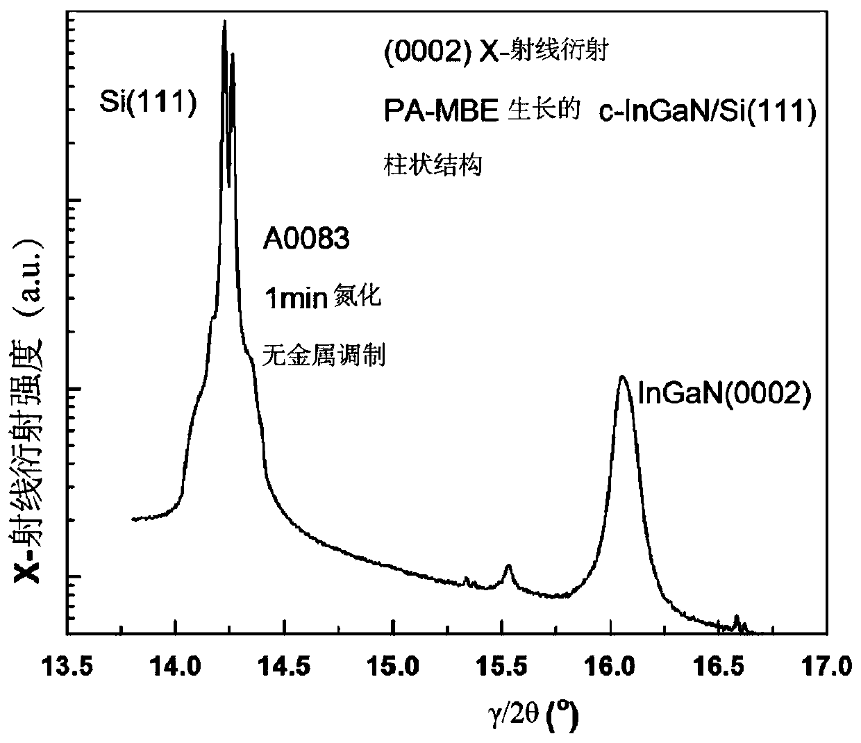
[0044] In this example, a three-dimensional dense layered structure composed of one-dimensional InGaN nanowires is prepared through the following steps:

[0045] 1) Provide a Si(111) substrate through nitriding treatment;

[0046] 2) On the Si(111) substrate, one-dimensional InGaN nanowires were epitaxially grown using plasma-assisted molecular beam epitaxy equipment (Vecco Gen II), and the specific settings were as follows:

[0047] Adjust the In / Ga total metal beam current to obtain a growth rate of about 0.5 μm / h;

[0048] By adjusting the In / Ga beam current ratio to 5 and the growth temperature at 450°C, the active N beam current is three times that of the metal In / Ga beam current.

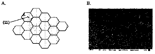
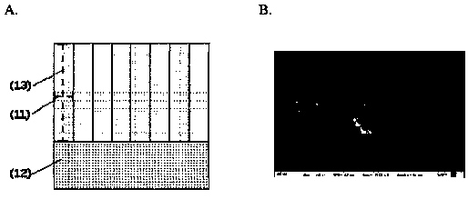
[0049] Through the above method, a three-dimensional dense InGaN structure (such as figure 1 with figure 2 As shown), the thickness of the InGaN three-dimensional dense structure is about 600nm.

[0050] figure 1 A is a top view of a schematic three-dimensional dense structure of InGaN, ...


PUM

PropertyMeasurementUnit
diameteraaaaaaaaaa
lengthaaaaaaaaaa
lengthaaaaaaaaaa

Abstract

The invention provides a nanowire array. All nanowires in the nanowire array are closely adhered, the nanowires make contact with each other through the side walls, and a three-dimensional dense layered structure is formed, wherein the nanowires are InGaN-based materials. The invention further provides an optoelectronic device with the nanowire array which is epitaxially grown on the substrate surface. The invention further provides a method for manufacturing the nanowire array and the optoelectronic device.

Description

technical field [0001] The invention relates to the field of semiconductor materials, in particular to a nanowire array, an optoelectronic device with the nanowire array and a manufacturing method thereof. Background technique [0002] One-dimensional nanoarrays and three-dimensional dense single crystal layers are often used in the epitaxial structure layer of semiconductor devices, especially for semiconductor optoelectronic devices such as light-emitting diodes, lasers, solar cells and high-power electronic amplifiers. Generally, the intrinsic properties of epitaxial layer materials used in optoelectronic devices require: low defect density, large active region volume, flexible heterostructure formation, simple preparation process, and stable lateral structure in the material layer. [0003] InGaN is an ideal material for optoelectronic devices. With the increase of In content, the bandgap of InGaN can be continuously adjusted from the ultraviolet band corresponding to G...

Claims


Application Information

Patent Timeline
Patent Type & Authority Applications(China)
IPC IPC(8): B82B1/00B82B3/00B82Y10/00B82Y40/00
CPCB81B2207/056B81C1/00031B82Y10/00B82Y20/00B82Y40/00H01L21/02381H01L21/02433H01L21/0254H01L21/02595H01L21/02603H01L21/02631H01L29/0676H01L29/2003H01L33/08H01L33/18H01L21/02378H01L21/02389H01L21/02395H01L21/0242
Inventor 理查德·内策尔王朋周国富斯特凡诺·桑吉内蒂
Owner SOUTH CHINA NORMAL UNIVERSITY
Why Eureka
Try Eureka