

Micro-nano wire manufacturing device and micro-nano structure
A technology for preparing devices and micro-nano structures, which is applied in the field of microelectronics, can solve the problems of complex process, small preparation area, and high cost, and achieve the effects of ensuring physical and chemical properties, low requirements for preparation conditions, and a wide range of options
- Summary
- Abstract
- Description
- Claims
- Application Information
AI Technical Summary
Problems solved by technology
Method used
Image

Examples
Embodiment 1
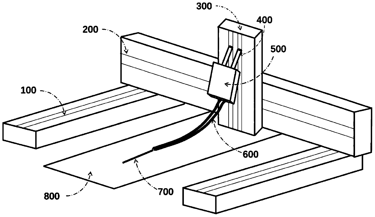
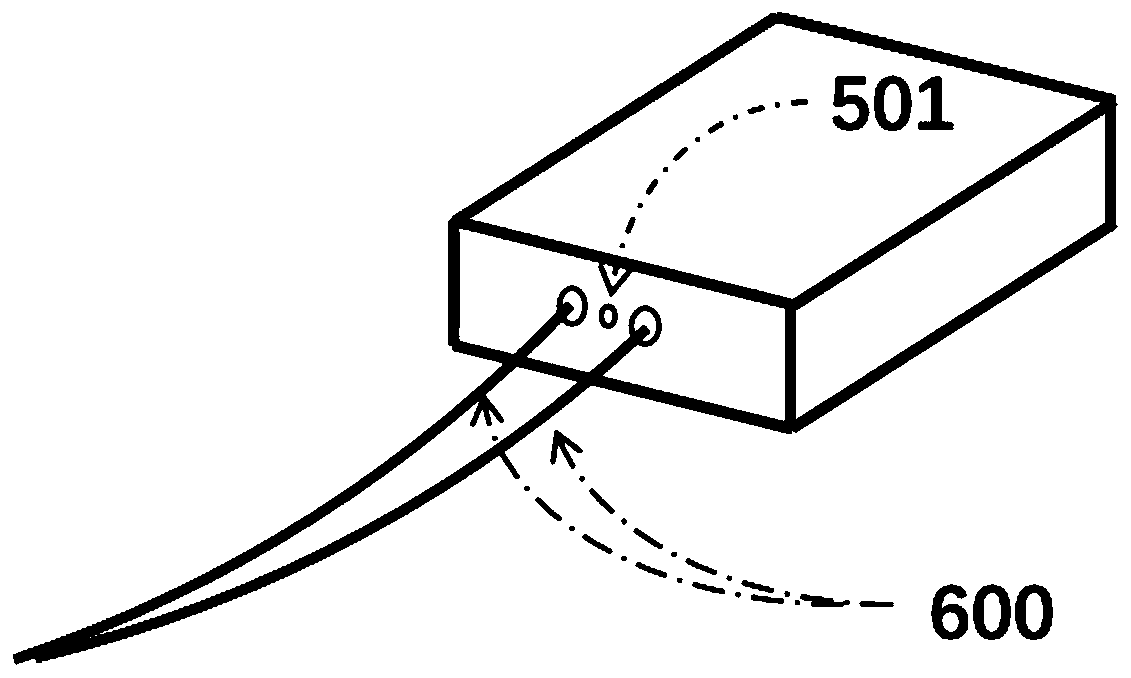
[0025] Such as figure 1 and figure 2 As shown, this embodiment relates to a micro-nano wire preparation device, including: a pair of X-axis linear displacement mechanism 100, Y-axis linear displacement mechanism 200, Z-axis linear displacement mechanism 300 and liquid-phase nanomaterial storage device 500, wherein, A substrate 800 is provided between a pair of X-axis linear displacement mechanisms 100; the liquid-phase nanomaterial storage device 500 is provided with a liquid outlet hole 501 and a micro-nano wire dispensing mechanism, and the micro-nano wire dispensing mechanism is set in one-to-one correspondence with the liquid outlet hole 501 The micro-nano wire application mechanism preferably includes two animal hairs 600, the roots of the two animal hairs 600 are preferably bonded on the liquid nanomaterial storage device 500, the liquid outlet 501 is arranged between the two animal hairs 600 roots, and the two animal hairs 600 The ends are drooping and lean against ea...
PUM
| Property | Measurement | Unit |
|---|---|---|
| Width | aaaaa | aaaaa |
| Thickness | aaaaa | aaaaa |
Abstract
Description
Claims
Application Information