A double-sided alignment process method for wafer processing
A process method and backside alignment technology, which is applied to the photolithography process of the patterned surface, instruments, semiconductor/solid-state device testing/measurement, etc., can solve the problem that the lithography machine cannot guarantee the alignment accuracy of the wafer, and achieve The effect of high precision and simple process method
- Summary
- Abstract
- Description
- Claims
- Application Information
AI Technical Summary
Problems solved by technology
Method used
Image

Examples
Embodiment 1
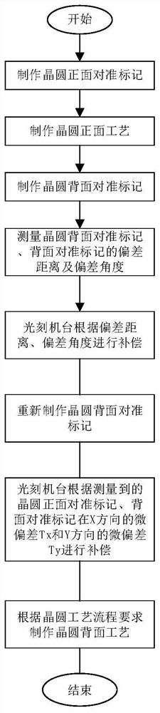
[0037] In Example 1, such as figure 1 As shown, a double-sided alignment process method for wafer processing is provided, which is especially suitable for a lithography machine without a double-sided alignment function to perform a double-sided process on a flat-edge wafer. The method specifically includes the following steps :
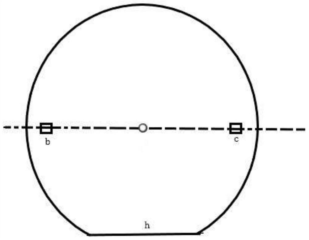
[0038] S01: Make the front alignment mark of the flat-edge wafer, and perform the front-side process of the flat-edge wafer; wherein, the production of the front-side alignment mark includes the center point of the flat-edge wafer parallel or perpendicular to the flat-edge wafer Two front alignment marks equidistant from the center of the wafer are set on the center line of the wafer on the flat side of the wafer. Such as figure 2 As shown, the flat-side wafer in the figure is a 6-inch flat-side wafer, b and c are the front alignment marks of the flat-side wafer, and h is the flat side of the flat-side wafer. More specifically, the front-side proc...
Embodiment 2
[0044] This implementation has the same inventive concept as Embodiment 1. On the basis of Embodiment 1, a double-sided alignment process method for wafer processing is provided, which is suitable for photolithography without double-sided alignment function. The machine performs double-sided process manufacturing on the non-flat wafer, and the method specifically includes the following steps:
[0045] S11: Make the front alignment mark of the non-flat wafer, and perform the front process of the non-flat wafer; wherein, the production of the front alignment mark includes selecting a non-flat edge of the non-flat wafer, connecting any non-flat Two points on the flat edge establish a virtual flat edge, such as Figure 4 The virtual flat edge h' in the virtual flat edge h' is parallel or perpendicular to the non-flat edge wafer center line that passes through the non-flat edge wafer center point, and the left and right two fronts that are equidistant from the wafer center are set ...
PUM
 Abstract
Description
Claims
Application Information
 - R&D
- Intellectual Property
- Life Sciences
- Materials
- Tech Scout
- Unparalleled Data Quality
- Higher Quality Content
- 60% Fewer Hallucinations
Browse by: Latest US Patents, China's latest patents, Technical Efficacy Thesaurus, Application Domain, Technology Topic, Popular Technical Reports.
© 2025 PatSnap. All rights reserved.Legal|Privacy policy|Modern Slavery Act Transparency Statement|Sitemap|About US| Contact US: help@patsnap.com