Three dimensional semiconductor memory device

A storage device and semiconductor technology, applied in the direction of semiconductor devices, semiconductor/solid-state device manufacturing, static memory, etc., can solve the problems of fine pattern formation technology level, increase the integration of two-dimensional or planar semiconductor devices, increase the fineness of patterns, etc.

Pending Publication Date: 2019-05-28
SAMSUNG ELECTRONICS CO LTD
View PDF8 Cites 4 Cited by
  • Summary
  • Abstract
  • Description
  • Claims
  • Application Information

AI Technical Summary

Problems solved by technology

As far as traditional two-dimensional or planar semiconductor devices are concerned, because their integration is mainly determined by the area occupied by a unit memory cell, integration is greatly affected by the level of

Method used


Image

  • Three dimensional semiconductor memory device
  • Three dimensional semiconductor memory device
  • Three dimensional semiconductor memory device

Examples


Embodiment Construction

[0016] Example embodiments will now be described more fully with reference to the accompanying drawings, in which example embodiments are shown.

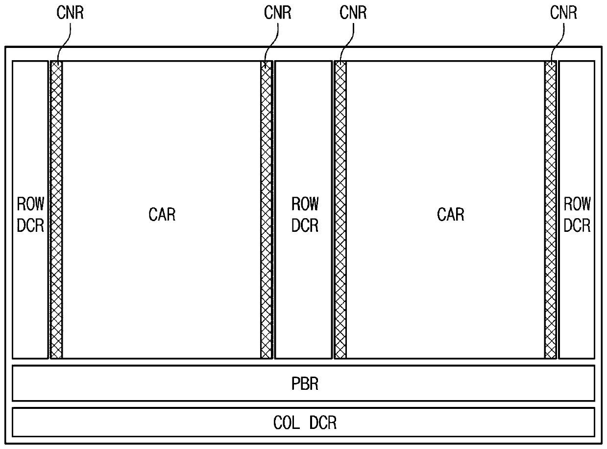
[0017] figure 1 is a diagram schematically showing the layout of a three-dimensional semiconductor memory device according to some embodiments.

[0018] refer to figure 1 , the three-dimensional semiconductor memory device may include a cell array region CAR and a peripheral circuit region. The peripheral circuit region may include a row decoder region ROW DCR, a page buffer region PBR, a column decoder region COL DCR, and a control circuit region (not shown). In some embodiments, a corresponding connection region CNR may be provided between the cell array region CAR and each row decoder region ROW DCR.

[0019] A memory cell array including a plurality of memory cells may be provided in the cell array area CAR. In some embodiments, the memory cell array may include a plurality of memory blocks, each of which is configured to in...


PUM


Abstract

Provided is a three-dimensional semiconductor memory device. The device may include a substrate that includes a cell array region and a connection region; an electrode structure provided on the substrate to extend in a first direction and include electrodes that are vertically stacked on the substrate and include pad portions which are stacked on the connection region to have a staircase structure; cell vertical structures provided on the cell array region to penetrate the electrode structure; dummy vertical structures provided on the connection region to penetrate the pad portion of each electrode; and cell contact plugs coupled to the pad portions of the electrodes. Each cell contact plug may have a non-circular top surface, and the dummy vertical structures may be arranged to surround each cell contact plug, in a plan view.

Description

technical field [0001] Exemplary embodiments relate to three-dimensional semiconductor memory devices, and in particular, to highly reliable and highly integrated three-dimensional semiconductor memory devices. Background technique [0002] Higher-integration semiconductor devices are required to meet consumer demand for superior performance and low price. In the case of a semiconductor device, increased integration is particularly important because its integration is an important factor in determining product prices. In the case of a conventional two-dimensional or planar semiconductor device, since its integration is mainly determined by the area occupied by a unit memory cell, the integration is greatly affected by the level of fine pattern formation technology. However, the extremely expensive process equipment required to increase pattern fineness sets practical limits to increasing the integration of two-dimensional or planar semiconductor devices. In order to overco...

Claims


Application Information

Patent Timeline
IPC IPC(8): H01L27/11524H01L27/11548H01L27/11556H01L27/1157H01L27/11575H01L27/11582
CPCG11C16/0483H10B43/10H10B43/40H10B43/35H10B43/27H01L21/76897H10B41/40H10B41/20H10B41/30G11C16/08
Inventor 甘喜星李太熙金敬勋
Owner SAMSUNG ELECTRONICS CO LTD
Why Eureka
Try Eureka