Check patentability & draft patents in minutes with Patsnap Eureka AI!

Lateral double diffused metal oxide semiconductor (ldmos) devices

A lateral double diffusion, semiconductor technology, used in semiconductor devices, electrical components, circuits, etc., can solve problems such as low switching time

Active Publication Date: 2022-05-17
格芯美国公司
View PDF4 Cites 0 Cited by
  • Summary
  • Abstract
  • Description
  • Claims
  • Application Information

AI Technical Summary

Problems solved by technology

However, to drive high-side power switches, the gate oxide of LDMOS must be thick enough to support high gate-source (Vgs) voltages, which is not possible with current fully depleted silicon-on-insulator (FDSOI) technology of
That is, there is no known high voltage (HV) LDMOS device in FDSOI capable of sustaining high Vgs and having low switching times

Method used


Image

  • Lateral double diffused metal oxide semiconductor (ldmos) devices
  • Lateral double diffused metal oxide semiconductor (ldmos) devices
  • Lateral double diffused metal oxide semiconductor (ldmos) devices

Examples


Embodiment Construction

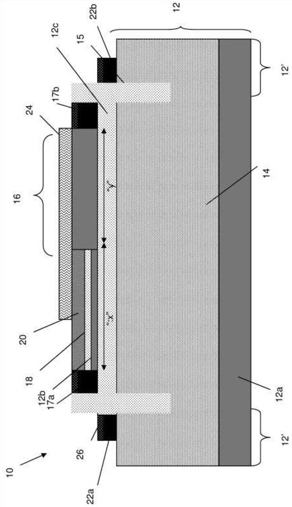
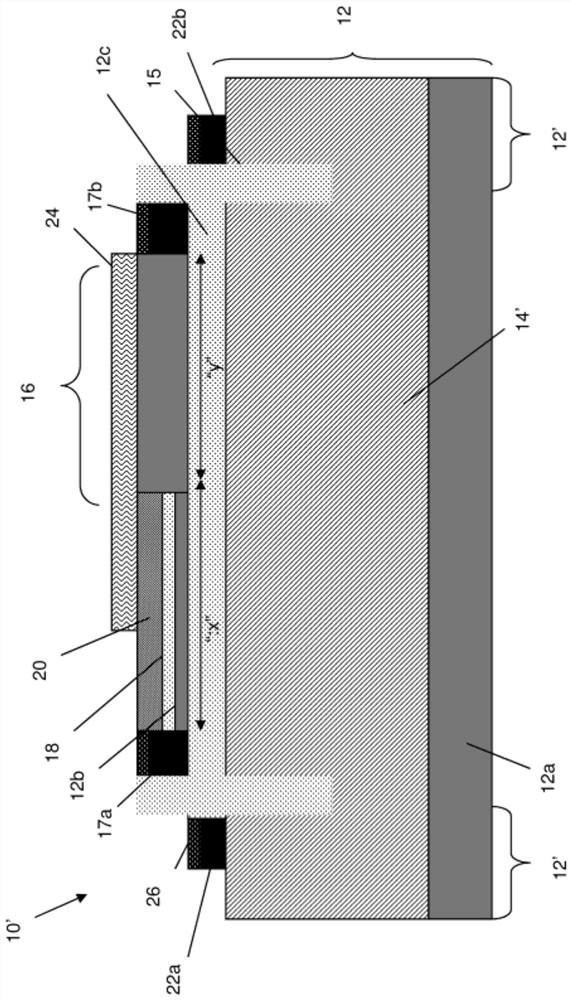
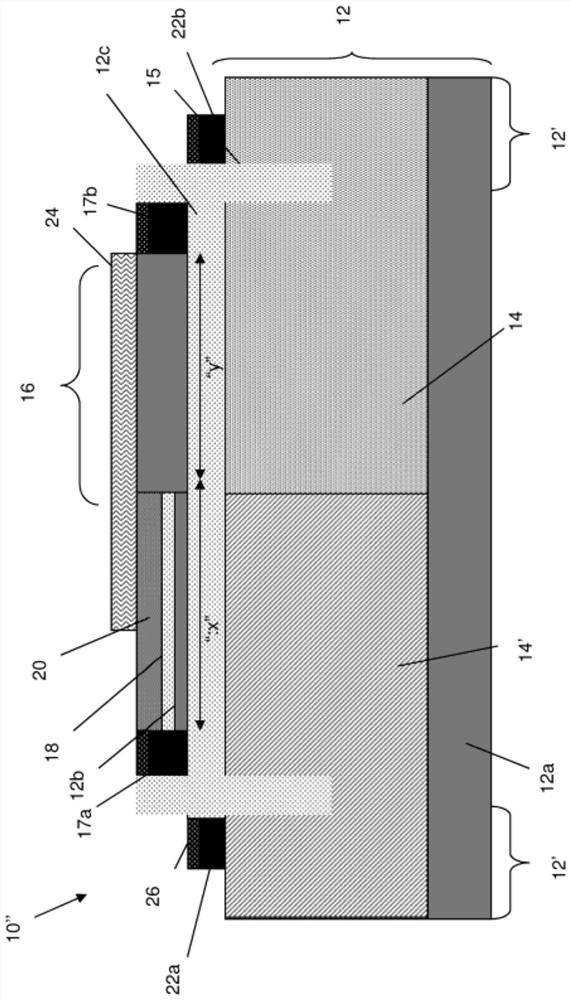
[0012] The present disclosure relates to semiconductor structures, and more particularly, to LDMOS devices on FDSOI structures and methods of fabrication. More specifically, this disclosure describes N-LDMOS or P-LDMOS devices on FDSOI that use a buried insulator layer (eg, a buried oxide layer) as the gate dielectric material. Advantageously, by implementing the structures described herein, LDMOS devices are capable of sustaining high input voltages, eg, high Vgs of 15V or higher, while also exhibiting low switching times.

[0013] The LDMOS structures of the present disclosure can be fabricated in a variety of ways using a variety of different tools. In general, methods and tools are used to form structures with micron and nanometer dimensions. The method for fabricating the LDMOS structure of the present disclosure, ie, technology, has been adopted from integrated circuit (IC) technology. For example, the structure can be built on a wafer and realized as a film of materia...


PUM

PropertyMeasurementUnit
thicknessaaaaaaaaaa
lengthaaaaaaaaaa

Abstract

The present invention relates to high input voltage enabled lateral double diffused metal oxide semiconductor (LDMOS) devices on fully depleted silicon on insulator (FDSOI). The present disclosure relates to semiconductor structures, and more particularly, to an LDMOS device on an FDSOI structure and a method of manufacturing the same. A lateral double-diffused semiconductor device comprising a gate dielectric composed of a buried insulator material of semiconductor-on-insulator (SOI) technology, a channel region composed of a semiconductor material of said SOI technology, and a source on the front side of said buried insulator / drain region such that the gate is formed on the backside of the buried insulator material. A gate terminal can also be placed at the hybrid portion to serve as a back gate voltage to control the channel and drift region of the device.

Description

technical field [0001] The present disclosure relates to semiconductor structures, and more particularly, to LDMOS devices on FDSOI substrates capable of sustaining high input voltages and methods of fabrication. Background technique [0002] In order to accommodate more and more high-voltage signal chip DC / DC converters, for example, automotive electronics or MEMS applications, there is a need for power ICs featuring thin / thick gate oxides and devices with higher voltage ratings Different process. High gate voltage capability is critical to achieve desired functionality in many application circuits such as display drivers or embedded flash drive circuits. [0003] Lateral double-diffused metal-oxide-semiconductor (LDMOS) devices are commonly used as power switches due to their compatibility with low-voltage CMOS in the same chip. However, to drive high-side power switches, the gate oxide of LDMOS must be thick enough to support high gate-source (Vgs) voltages, which is no...

Claims


Application Information

Patent Timeline
Patent Type & Authority Patents(China)
IPC IPC(8): H01L29/78H01L29/06
CPCH01L29/78624H01L29/7824H01L29/0886H01L29/42364H01L29/42372H01L29/402H01L29/66681H01L29/0873H01L29/42376
Inventor I·C·马约尔A·扎卡T·赫尔曼E·M·巴齐齐
Owner 格芯美国公司
Features
  • R&D
  • Intellectual Property
  • Life Sciences
  • Materials
  • Tech Scout
  • Unparalleled Data Quality
  • Higher Quality Content
  • 60% Fewer Hallucinations
Learn More