A Method for Fabricating Two-Dimensional Flexible Light-Emitting Arrays Using Local Stress

A light-emitting array and local stress technology, which is applied in the direction of semiconductor devices, electrical components, circuits, etc., can solve problems such as the inability to control the light-emitting parts of devices, and achieve the effect of meeting technical requirements

Active Publication Date: 2021-03-02
SHANGHAI UNIVERSITY OF ELECTRIC POWER
View PDF5 Cites 0 Cited by
  • Summary
  • Abstract
  • Description
  • Claims
  • Application Information

AI Technical Summary

Problems solved by technology

However, if this light-emitting device wants to emit light, the energy of the irradiated light must be greater than the forbidden band width; and because the device material has the same forbidden band width and the same light-emitting conditions, it is impossible to control the light-emitting part of the device.

Method used


Image

  • A Method for Fabricating Two-Dimensional Flexible Light-Emitting Arrays Using Local Stress

Examples


Embodiment 1

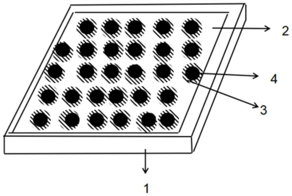
[0030] A method for preparing a two-dimensional flexible light-emitting array using local stress, comprising the following steps:

[0031] (1) Using flexible materials as the substrate;

[0032] (2) Depositing a layer of metal material on the substrate;

[0033] (3) carrying out microwave annealing to the substrate after depositing the metal material in step (2), so that the metal material forms metal islands on the substrate;

[0034] (4) Continue to transfer a layer of tungsten diselenide layer on the metal island formed in step (3), which is completed.

[0035] In this embodiment, in step (1), the flexible material is polyimide. In step (2), the metal material is gold with a thickness of 20-50nm. In step (3), the process conditions of microwave annealing are: microwave power 2000-5000 watts, annealing time 1-10 minutes. . In step (4), the thickness of the tungsten diselenide layer is two atomic layers.

Embodiment 2

[0037] Compared with Embodiment 1, most of them are the same, except that in this embodiment, the flexible material is polyethylene naphthalate.

Embodiment 3

[0039] Compared with Embodiment 1, most of them are the same, except that in this embodiment, the flexible material is polyethylene terephthalate.


PUM

PropertyMeasurementUnit
thicknessaaaaaaaaaa

Abstract

The invention relates to a method for preparing a two-dimensional flexible light-emitting array by using local stress, comprising the following steps: (1) using a flexible material as a substrate; (2) depositing a layer of metal material on the substrate; (3) performing the steps of ( 2) Microwave annealing is carried out on the substrate after depositing the metal material, so that the metal material forms a metal island on the substrate; (4) continue to transfer a layer of tungsten diselenide layer on the metal island formed in step (3), that is, complete . Compared with the prior art, the present invention can realize the control and selection of the light-emitting units in the light-emitting array, and at the same time, the device can be bent and folded at will, and the electrical performance of the device remains unchanged after bending, which satisfies certain limits or special conditions. Under the application requirements, it can also meet the technical requirements of portable electronic products for miniaturized power supplies.

Description

technical field [0001] The invention belongs to the technical field of flexible electronic preparation, and relates to a method for preparing a two-dimensional flexible light-emitting array by using local stress. Background technique [0002] Semiconductor optoelectronic device refers to a new type of semiconductor device that connects the two physical quantities of light and electricity to convert light and electricity into each other. That is, devices made using the photoelectric effect (or thermoelectric effect) of semiconductors. However, if this light-emitting device wants to emit light, the energy of the irradiated light must be greater than the forbidden band width; and because the device material has the same forbidden band width and the same light-emitting conditions, it is impossible to control the light-emitting part of the device. As disclosed in Chinese patent ZL201510016315.X, a flexible light-emitting device array and its manufacturing method include: a plura...

Claims


Application Information

Patent Timeline
Patent Type & Authority Patents(China)
IPC IPC(8): H01L33/00H01L33/26H01L27/15
Inventor 汤乃云张伟
Owner SHANGHAI UNIVERSITY OF ELECTRIC POWER
Why Eureka
Try Eureka