Method for preparing in-situ transmission electron microscope sample based on heated chip

A technology for TEM samples and heating chips, applied in the preparation of test samples, metal processing equipment, electron beam welding equipment, etc., can solve problems such as sample damage, improve yield, increase sample preparation efficiency, and ensure sample quality. Effect

Inactive Publication Date: 2019-05-31
MATERIAL INST OF CHINA ACADEMY OF ENG PHYSICS
View PDF8 Cites 12 Cited by
  • Summary
  • Abstract
  • Description
  • Claims
  • Application Information

AI Technical Summary

Problems solved by technology

For example, Pt is not used to protect the required sample during initial cutting sampling, which may easily lead to damage to the sample by Ga ion implantation, especially for materials that are sensitive

Method used


Image

  • Method for preparing in-situ transmission electron microscope sample based on heated chip
  • Method for preparing in-situ transmission electron microscope sample based on heated chip
  • Method for preparing in-situ transmission electron microscope sample based on heated chip

Examples


preparation example Construction

[0048] figure 1 A flow chart showing a heating chip-based in-situ transmission electron microscope sample preparation method according to an exemplary embodiment of the present invention, as figure 1 As shown, according to an exemplary embodiment of the present invention, the heating chip-based in-situ TEM sample preparation method mainly includes the following steps.

[0049] Step A:

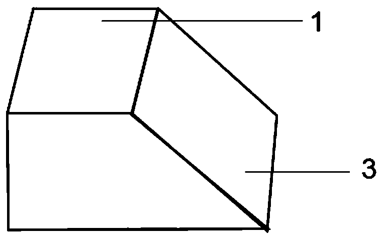
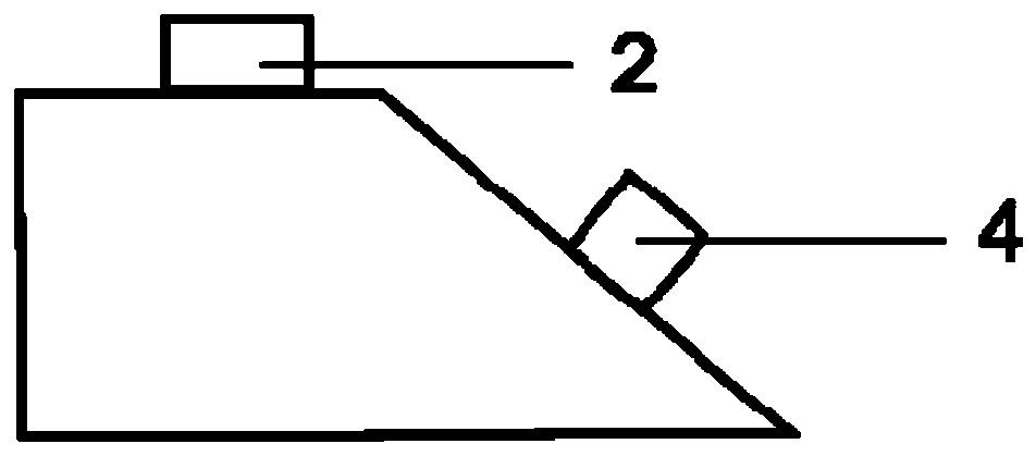
[0050] The initial sample 2 and the heating chip 4 are respectively fixed on the adjacent plane 1 and slope 2 on the prefabricated sample stage 11, and then the prefabricated sample stage 11 is transferred to the FIB-SEM dual-beam system and vacuumized.

[0051] Figure 2a It shows a schematic structural view of the prefabricated sample stage in the in-situ transmission electron microscope sample preparation method based on the heating chip according to an exemplary embodiment of the present invention, Figure 2b A schematic diagram showing the position of the initial sample and the heating ...

Embodiment 1

[0087] Figure 7a Showing the microscopic topography figure of depositing the Pt protection layer on the initial sample in embodiment 1, Figure 7b It shows the microscopic topography diagram of etching a deep groove at one end edge of the Pt protective layer of the initial sample deposited with the Pt protective layer in Example 1, Figure 7c Shown in embodiment 1 in the initial sample that is deposited with Pt protection layer, the microcosmic topography figure of one side etching cutting of strip sample is carried out on one side edge of Pt protection layer, Figure 7d It shows the microscopic topography diagram of etching and cutting the other side of the strip sample at the edge of the other side of the Pt protective layer of the initial sample deposited with the Pt protective layer in Example 1, Figure 7e Shown in embodiment 1 is adjusted the microscopic topography figure that the strip sample surface is perpendicular to the ion beam direction, Figure 7f Showing the...

Embodiment 2

[0102] Figure 10a A microscopic topography diagram of etching a deep groove at one end edge of the Pt protective layer of the initial sample deposited with the Pt protective layer in Example 2 is shown, Figure 10b Shown in embodiment 2 is deposited on the Pt protective layer side edge of the initial sample of Pt protective layer and carries out the microscopic topography figure of one side etching cutting of strip sample, Figure 10c Shown in embodiment 2 in the other side edge of the Pt protective layer of the initial sample deposited with the Pt protective layer, the microscopic topography of the other edge of the strip sample is etched and cut, Figure 10d The microscopic topography diagram of adjusting the surface of the strip sample perpendicular to the direction of the ion beam in Example 2 is shown.

[0103] In this embodiment, aluminum (Al) thin film is selected as the material for preparing the sample, and the in-situ heating TEM sample is prepared based on the in-...


PUM

PropertyMeasurementUnit
Thicknessaaaaaaaaaa
Thicknessaaaaaaaaaa
Etching depthaaaaaaaaaa

Abstract

The invention discloses a method for preparing in-situ transmission electron microscope (TEM) sample based on a heated chip. The method comprises a step of fixing an initial sample and a heated chip to adjacent plane and inclined surface on a prefabricated sample table, then transferring the initial sample and the heated chip into a FIB-SEM double-beam system and performing vacuuming, a step of depositing a Pt protective layer on the surface of the initial sample by using an ion beam to obtain the initial sample deposited with the Pt protective layer, a step of cutting the initial sample deposited with the Pt protective layer by an ion beam to obtain a strip sample with a triangular cross section, a step of transferring the strip sample and fixing the strip sample to a sample hole groove of the heated chip by using a mechanical hand, and a step of adjusting the position of the prefabricated sample table and stepwise thinning the strip sample by an ion beam to obtain the in-situ transmission electron microscope sample based on the heated chip. According to the invention, the preparation of the in-situ TEM sample is carried out by using the FIB-SEM double-beam system, only one time of sample introduction is needed, the process flow is greatly simplified, the operation is simple and intuitive, and the improvement of the yield of sample preparation is improved.

Description

technical field [0001] The invention belongs to the field of electronic microscopic analysis of materials, and relates to a preparation method of an in-situ heated transmission electron microscope (TEM) sample, in particular to a focused ion beam (FIB) processing method of an in-situ transmission electron microscope sample based on a heating chip. Background technique [0002] The in-situ transmission electron microscope (TEM) characterization method can be used to analyze the change law of the internal structure of the material with temperature, and obtain the physical law of the change of the material microstructure with the external environment. High-quality in-situ TEM experimental samples are the prerequisite for in-situ TEM characterization. In-situ heating TEM experiments are generally based on in-situ heating of the chip, which requires the sample to be fixed on the chip and then thinned to a thickness of less than 100 nanometers. After the sample preparation is com...

Claims


Application Information

Patent Timeline
IPC IPC(8): G01N1/28G01N1/44B23K10/00B23K15/08
Inventor 路超曾荣光张厚亮赵雅文廖益传陈丕恒
Owner MATERIAL INST OF CHINA ACADEMY OF ENG PHYSICS
Why Eureka
Try Eureka