Method for correcting a mask layout and method of fabricating a semiconductor device using the same

A mask and layout technology, applied in the field of correcting mask layout and using it to manufacture semiconductor devices, to achieve the effect of compensating for deformation

Pending Publication Date: 2019-05-31
SAMSUNG ELECTRONICS CO LTD
View PDF5 Cites 0 Cited by
  • Summary
  • Abstract
  • Description
  • Claims
  • Application Information

AI Technical Summary

Problems solved by technology

Due to this proximity, interference and diffraction of light may occur, so a distorted layout different from the desired layout may be printed on the wafer

Method used


Image

  • Method for correcting a mask layout and method of fabricating a semiconductor device using the same
  • Method for correcting a mask layout and method of fabricating a semiconductor device using the same
  • Method for correcting a mask layout and method of fabricating a semiconductor device using the same

Examples


Embodiment Construction

[0018] Hereinafter, embodiments of the inventive concept will be described in detail with reference to the accompanying drawings.

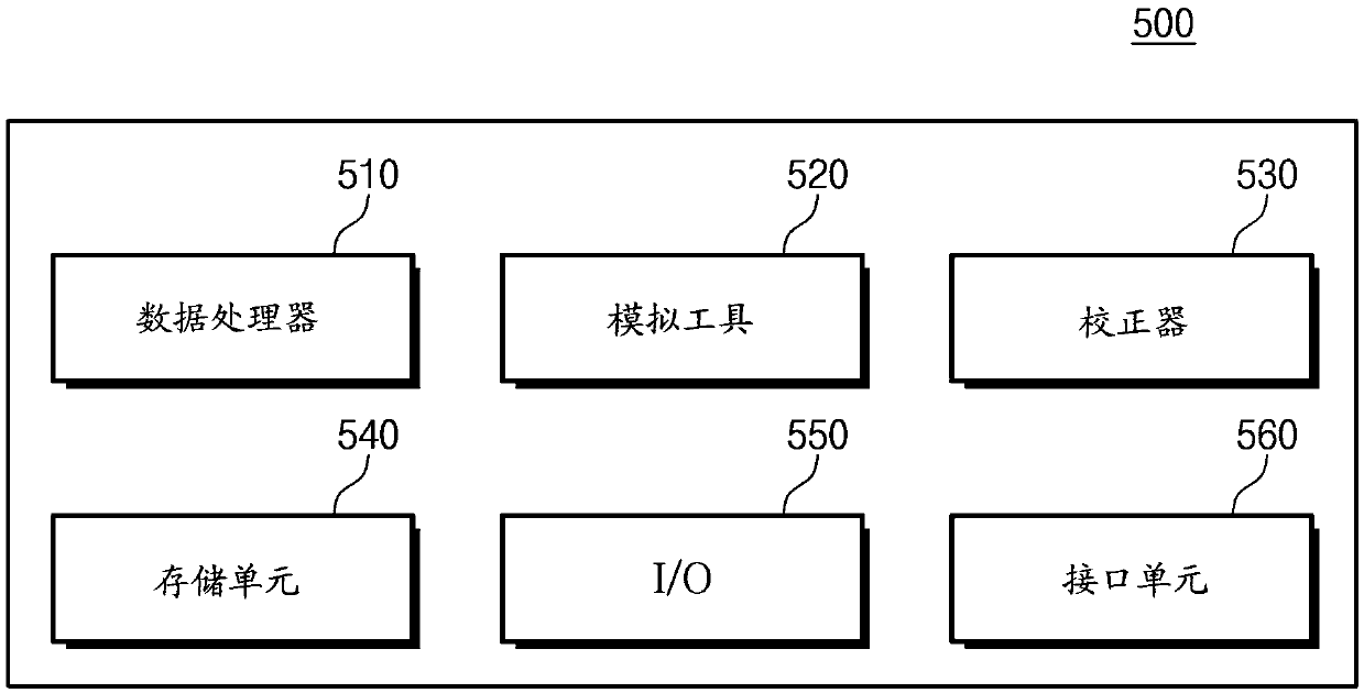
[0019] figure 1 is a schematic block diagram illustrating a computer system for performing a method of correcting a mask layout according to some embodiments of the inventive concepts.

[0020] refer to figure 1 , the computer system 500 may include a data processor 510 for processing various data, a simulation tool 520 for performing lithography simulations on the designed mask layout, and a corrector 530 that compares The generated data is compared with the expected data and the mask layout is corrected when the difference between the generated data and the expected data exceeds the allowable range. The computer system 500 may also include a storage unit 540 capable of storing various data. The storage unit 540 may include a hard disk and / or a nonvolatile semiconductor memory device (eg, a flash memory device, a phase change memory device, an...


PUM


Abstract

The invention relates to a method for correcting a mask layout and a method of fabricating a semiconductor device using the same. The method for correcting a mask layout includes providing a mask layout including first patterns, each of the first patterns having a size related to a first critical dimension (CD) value, obtaining topography data on a region of a wafer, generating a defocus map usingthe topography data, and correcting the mask layout on the basis of the defocus map. The generating of the defocus map includes respectively setting second CD values for a plurality of sub-regions ofthe mask layout. The second CD values may be set based on the topography data. The correcting of the mask layout on the basis of the defocus map comprises correcting the sizes of the first patterns to be related to the second CD values.

Description

technical field [0001] Embodiments of the inventive concept relate to a method for correcting a mask layout designed for manufacturing a photomask and a method of manufacturing a semiconductor device using the mask layout. Background technique [0002] Photomasks may be used to print integrated circuit layouts on wafers in the photolithographic process used to fabricate semiconductor devices. Generally, a photolithography process may use a method of transferring a mask pattern formed on a photomask to a wafer through an optical lens. A photomask can include transparent regions and opaque regions. The transparent region can be formed by etching a metal layer disposed on the photomask, and can transmit light. Opaque areas, on the other hand, may not transmit light. The mask pattern may be formed of transparent regions and opaque regions. Light emitted from a light source can be irradiated to a wafer through a mask pattern of a photomask, so that an integrated circuit layou...

Claims


Application Information

Patent Timeline
IPC IPC(8): G03F1/42G03F1/36H01L21/027
CPCG03F1/70G03F1/36G03F7/70441G03F7/705H01L21/0274G03F7/70625
Inventor 文晟墉李受龙金昌焕
Owner SAMSUNG ELECTRONICS CO LTD
Why Eureka
Try Eureka