Cleaning method of grinded silicon wafer

A silicon wafer cleaning and pre-cleaning technology, applied in electrical components, semiconductor/solid-state device manufacturing, circuits, etc., can solve the problems affecting the service life of the cleaning machine, wasted thickness of silicon wafer raw materials, and short cleaning life, so as to save manufacturing costs. As well as the later detection and maintenance costs, reducing the harm of ultrasound to the human body, and improving the effect of cleanliness

Active Publication Date: 2019-06-07
TIANJIN ZHONGHUAN ADVANCED MATERIAL TECH +1
View PDF6 Cites 5 Cited by
  • Summary
  • Abstract
  • Description
  • Claims
  • Application Information

AI Technical Summary

Problems solved by technology

[0005] Ultrasonic cleaning process principle: use ultrasonic cavitation to remove the adsorbed impurities on the surface of the silicon wafer, and then use the cleaning liquid complexation to absorb the impurities to achieve the purpose of cleaning; there are problems of weak cleaning ability and short cleaning life;
[0006] The principle of micro-etching cleaning process: use concentrated alkali to etch silicon wafers, remove impurities on the surface of silicon wafers and at the same time remove the oxide layer of silicon wafers and the silicon wafer itself; there is a waste of silicon wafer raw materials (the loss of its own thickness), which affects the service life of the cleaning machine The problem

Method used


Image

  • Cleaning method of grinded silicon wafer
  • Cleaning method of grinded silicon wafer
  • Cleaning method of grinded silicon wafer

Examples


Embodiment Construction

[0033] Unless otherwise defined, the technical terms used in the following embodiments have the same meaning as commonly understood by those skilled in the art to which the present invention belongs. The test reagents used in the following examples, unless otherwise specified, are conventional biochemical reagents; the experimental methods, unless otherwise specified, are conventional methods.

[0034] The present invention will be described in detail below in conjunction with examples.

[0035] The purpose of this process is to remove impurities such as corundum, silicon powder, silicon oxide, and metal oxide remaining on the surface of the ground silicon wafer.

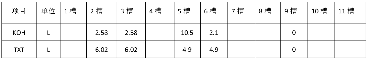
[0036] It includes pre-cleaning and cleaning steps in sequence, wherein the pre-cleaning sequentially includes bubbling, pre-cleaning solution cleaning and pure water cleaning; cleaning includes ultrasonic cleaning and pure water cleaning, wherein ultrasonic cleaning and pure water cleaning Alternate several times....


PUM


Abstract

The present invention provides a cleaning method of a grinded silicon wafer. The method comprises the steps of, in order: a pre-cleaning step and a cleaning step. The pre-cleaning comprises the stepsin order: bubbling blow washing, cleaning with a pre-cleaning liquid and cleaning with pure water; and the cleaning comprises the steps of: cleaning free of the ultrasound medicine liquid and cleaningwith pure water, wherein the cleaning free of the ultrasound medicine liquid and the cleaning with pure water are alternately performed for many times. The cleaning method of the grinded silicon wafer omits concentrated alkaline and ultrasound, the silicon wafer is rotated in the dilute alkalis and the cleaning liquid driven by a roller to strip off the impurities at the surface of the silicon wafer.

Description

technical field [0001] The invention belongs to the field of semiconductor manufacturing, and in particular relates to a cleaning process for a polished silicon wafer. Background technique [0002] The preparation of silicon materials includes directional cutting, grinding, polishing, etc. Grinding is performed after slicing. Since the silicon single wafer after slicing does not yet have the curvature, flatness and parallelism required in the semiconductor manufacturing process, grinding This step has become a key process for effectively improving the curvature, flatness and parallelism of silicon single wafers. [0003] However, there are residues on the surface of the ground silicon wafer, including corundum, silicon powder, silicon oxide and metal oxide. Before the next step of processing, the residue on the surface needs to be cleaned. [0004] The existing cleaning processes are mainly ultrasonic cleaning process and micro corrosion cleaning process. [0005] Ultraso...

Claims


Application Information

Patent Timeline
Patent Type & Authority Applications(China)
IPC IPC(8): H01L21/02H01L21/67
Inventor 张堪由佰玲苏荣义白玉麟徐荣清王彦君
Owner TIANJIN ZHONGHUAN ADVANCED MATERIAL TECH
Why Eureka
Try Eureka