Piezoelectric acoustic wave filter

A piezoelectric sound wave and filter technology, applied in the direction of electric solid devices, circuits, electrical components, etc., can solve the problems affecting the out-of-band suppression of the filter, and achieve the effect of height reduction and small inductance

Active Publication Date: 2019-06-07
TIANJIN UNIV +1
View PDF2 Cites 15 Cited by
  • Summary
  • Abstract
  • Description
  • Claims
  • Application Information

AI Technical Summary

Problems solved by technology

[0005] However, there is a technical problem that is not easy to solve in the bonding micro-assembly of BAW: all bonding wires can be equivalent to an inductance of about 0.3nH ~ 1nH, and for radio frequency devices, whether it is a signal wire or a ground wire, there must be The coupling between inductors, that is, mutual inductance
This mutual inductance will have a greater impact on the characteristics of the filter, generally affecting the position of the out-of-band transmission zero, thus affecting the out-of-band rejection of the filter

Method used


Image

  • Piezoelectric acoustic wave filter
  • Piezoelectric acoustic wave filter
  • Piezoelectric acoustic wave filter

Examples


Embodiment 1

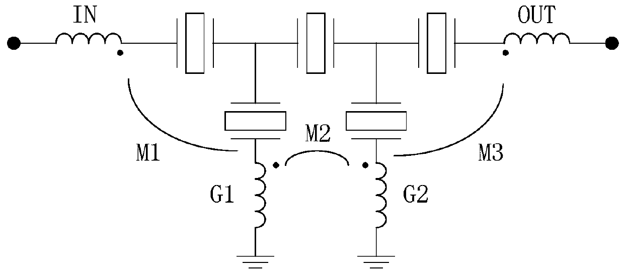
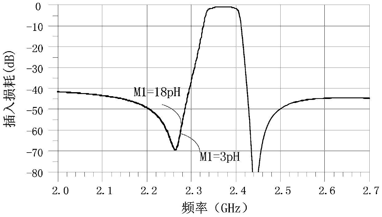
[0031] Figure 4a and 4b It is a structural diagram of the implementation of a piezoelectric acoustic wave filter, Figure 4b The two signals of IN and OUT in the middle are connected to the series resonator, and are conducted to the bonding pad on the upper surface of the upper wafer through the via hole of the upper wafer. The bonding pad or transmission line on the board; the two grounds of G1 and G2 are connected to the parallel resonator, and are connected to the metallization plane on the lower surface of the lower wafer through the via hole of the lower wafer. Such as Figure 4a and 4b As shown, the piezoelectric acoustic wave filter includes a carrier board 1 and a chip on the carrier board 1 consisting of an upper wafer 4 and a lower wafer 5, and an input signal bonding pad is arranged on the upper surface of the upper wafer 4 Chip 3 and output signal bonding gasket 11, input signal bonding finger 2 and output signal bonding finger 12 are arranged on the carrier boa...

Embodiment 2

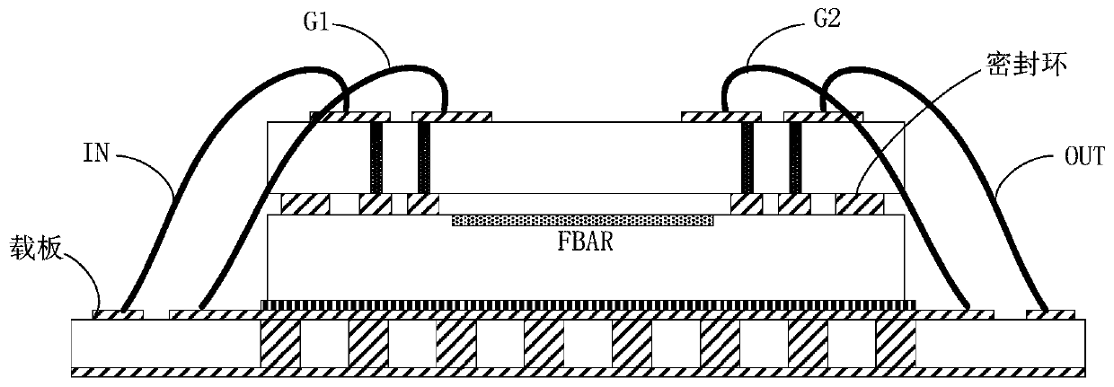
[0038] Figure 5 It is the structural diagram of the second piezoelectric acoustic wave filter in this implementation. Such as Figure 5 As shown, the piezoelectric acoustic wave filter includes a carrier board 1 and a chip on the carrier board 1 consisting of an upper wafer 4 and a lower wafer 5, and an input signal bonding pad is arranged on the upper surface of the upper wafer 4 Chip 3 and output signal bonding gasket 11, input signal bonding finger 2 and output signal bonding finger 12 are arranged on the carrier board 1; a sealing ring 7 is arranged between the upper wafer 4 and the lower wafer 5 for Enclose sensitive circuits between two wafers.

[0039] The upper wafer 4 is provided with two via holes 10, and the lower wafer 5 is also provided with two via holes 10; the input signal line is connected to the upper surface of the upper wafer through a via hole in the upper wafer 4 The input signal bonding pad 3; the output signal lines are respectively connected to the...

Embodiment 3

[0045] Figure 6a and 6b is the structural diagram of the implementation of the triple piezoelectric acoustic wave filter, where Figure 6b The dotted box indicates the contour edge on the wafer. Such as Figure 6a and 6b As shown, the piezoelectric acoustic wave filter includes a carrier plate 1 and an upper wafer 4 and a lower wafer 5 arranged from top to bottom on the carrier plate 1, and the upper wafer 4 and the lower wafer 5 are provided with The sealing ring 7 is used to seal the sensitive circuit between two wafers; the upper surface of the lower wafer 5 is provided with an input signal bonding pad 3 and an output signal bonding pad 11, and the carrier board 1 An input signal bonding finger 2 and an output signal bonding finger 12 are provided.

[0046] The lower wafer 5 is provided with two via holes 10; the sealing ring 7 is provided with an opening, and the input signal line passes through the opening on the sealing ring and is connected to the input signal bon...


PUM


Abstract

The invention provides a piezoelectric acoustic wave filter, which realizes high performance and high consistency of a piezoelectric acoustic wave filter device under a micro-assembly condition. The piezoelectric acoustic wave filter comprises a carrier plate, an upper wafer and a lower wafer, wherein the upper wafer and the lower wafer are located on the carrier plate and sequentially arranged from top to bottom, wherein the upper wafer and the lower wafer are respectively provided with a plurality of via holes, or only the lower wafer is provided with a plurality of via holes; alternatively,the piezoelectric acoustic wave filter comprises a carrier plate and a first wafer, a second wafer and a third wafer which are located on the carrier plate and arranged from top to bottom, and a plurality of via holes are formed in the second wafer and the third wafer respectively.

Description

technical field [0001] The invention relates to the field of filtering devices for communication, in particular to a piezoelectric acoustic wave filter which is manufactured using the principle of piezoelectric effect and can be assembled by gold wire bonding. Background technique [0002] At present, the small-sized filter devices that can meet the needs of communication terminals are mainly piezoelectric acoustic wave filters. The resonators that make up this type of acoustic wave filter mainly include: FBAR (Film Bulk Acoustic Resonator, thin film bulk acoustic resonator), SMR (Solidly Mounted Resonator, solid-state assembly resonator) and SAW (Surface AcousticWave, surface acoustic wave resonator). Among them, filters based on the principle of bulk acoustic wave FBAR and SMR (collectively referred to as BAW, bulk acoustic wave resonator), compared with filters based on the principle of surface acoustic wave SAW, have lower insertion loss, faster roll-off characteristics ...

Claims


Application Information

Patent Timeline
Patent Type & Authority Applications(China)
IPC IPC(8): H03H9/58H03H9/17
CPCH03H9/0547H03H9/1014H03H9/0533H03H9/0514H01L2224/48145H01L2224/45144H01L24/45H01L2224/48091H01L2224/32225H01L2224/73257H01L2224/73253H01L2224/05569H01L2224/83194H01L2224/32145H01L2224/48227H01L2224/16145H01L24/05H01L2224/16146H01L2224/0557H01L2224/04042H01L24/48H01L24/16H01L24/32H01L24/29H01L24/83H01L2224/8385H01L2924/0781H01L24/73H01L2224/85399H01L2224/29099H01L2224/13099H01L2224/83399H01L2224/05599H01L2924/00014
Inventor 庞慰郑云卓
Owner TIANJIN UNIV
Why Eureka
Try Eureka