Thermal control skin capable of adjusting equivalent emissivity by voltage and application thereof in spacecraft

A technology of equivalent emissivity and voltage adjustment, which is applied in the fields of instruments, optics, nonlinear optics, etc., can solve the problems of poor chemical stability, inability to withstand erosion, and small range of material choices, achieving large degrees of freedom and high spatial stability , to ensure the effect of space stability

Active Publication Date: 2019-06-11
HARBIN INST OF TECH
View PDF8 Cites 10 Cited by
  • Summary
  • Abstract
  • Description
  • Claims
  • Application Information

AI Technical Summary

Problems solved by technology

[0003] Although the electrochromic thermal control has a wide range of emissivity adjustment, electrochromic materials must be used, and the selection range of materials is small
Moreover, many electrochromic mate

Method used


Image

  • Thermal control skin capable of adjusting equivalent emissivity by voltage and application thereof in spacecraft
  • Thermal control skin capable of adjusting equivalent emissivity by voltage and application thereof in spacecraft
  • Thermal control skin capable of adjusting equivalent emissivity by voltage and application thereof in spacecraft

Examples


Embodiment 1

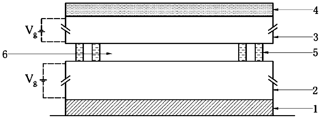
[0061] A thermal control skin, comprising base 1, inner layer 2, outer layer 3 and optical solar reflector 4 from bottom to top, with spacer 5 between inner layer 2 and outer layer 3, said spacer 5 makes inner layer 2 A vacuum gap 6 is formed between the outer layer 3 and the outer layer 3, and the inner layer 2 is a metal-insulator-semiconductor structure.

[0062] Specifically, the material of substrate 1 is SiO 2 ; The inner layer 2 is a metal-insulator-semiconductor structure, the metal layer in the structure is an Ag film with a thickness of 1 μm, the insulator layer is a SiC film with a thickness of 1 μm, and its breakdown voltage is 300V, and the semiconductor layer is an ITO film with a thickness of 10nm, and the semiconductor layer in the structure is adjacent to the vacuum gap 6, and a forward DC adjustable voltage is applied between the semiconductor layer and the metal layer; the outer layer 3 is a 10μm thick Al film substrate + a 10nm thick ITO film, coated on an ...

Embodiment 2

[0065] A thermal control skin, comprising base 1, inner layer 2, outer layer 3 and optical solar reflector 4 from bottom to top, with spacer 5 between inner layer 2 and outer layer 3, said spacer 5 makes inner layer 2 A vacuum gap 6 is formed between the outer layer 3 and the outer layer 3, and the inner layer 2 is a metal-insulator-semiconductor structure.

[0066] Specifically, the material of substrate 1 is SiO 2 ; The inner layer 2 is a metal-insulator-semiconductor structure, the metal layer in the structure is an Ag film with a thickness of 1 μm, the insulator layer is a SiC film with a thickness of 1 μm, and its breakdown voltage is 300V, and the semiconductor layer is an ITO film with a thickness of 10nm, and the semiconductor layer in the structure is adjacent to the vacuum gap 6, and a forward DC adjustable voltage is applied between the semiconductor layer and the metal layer; the outer layer 3 is a 10μm thick Al film substrate + a 10nm thick p-type doped silicon fi...

Embodiment 3

[0069] A thermal control skin, comprising base 1, inner layer 2, outer layer 3 and optical solar reflector 4 from bottom to top, with spacer 5 between inner layer 2 and outer layer 3, said spacer 5 makes inner layer 2 A vacuum gap 6 with a pitch of micronano scale is formed between the outer layer 3 and the outer layer 3 is a metal-insulator-semiconductor structure.

[0070] Specifically, the material of substrate 1 is SiO 2 The inner layer 2 is a 10 μm thick Al substrate+10nm thick ITO film; the outer layer 3 is a metal-insulator-semiconductor structure, and the metal layer in the structure is an Ag film with a thickness of 1 μm, which is coated on the inner surface of the optical solar mirror 5, and the insulator The layer is a SiC film with a thickness of 1 μm, its breakdown voltage is 300V, the semiconductor layer is an ITO film with a thickness of 10nm, and the semiconductor layer in the structure is adjacent to the vacuum gap 6, and a positive direct current can be added...


PUM

PropertyMeasurementUnit
Thicknessaaaaaaaaaa
Breakdown electricityaaaaaaaaaa
Thicknessaaaaaaaaaa

Abstract

The present invention relates to a thermal control skin capable of adjusting equivalent emissivity by voltage and an application thereof in a spacecraft. The thermal control skin comprises a substrate, an inner layer, an outer layer and a protecting layer from bottom to top, and a spacer is arranged between the inner layer and the outer layer. The spacer forms a vacuum gap with a spacing of micro-nano scale between the inner layer and the outer layer. The inner layer and/or the outer layer comprises a metal-insulator-semiconductor structure, and direct current adjustable voltage is loaded between the semiconductor and the metal in the structure. The protecting layer has high infrared emissivity or both high infrared emissivity and low solar spectral absorptivity. On one hand, the thermal control skin has good adaptability to a space environment, and solves the problem of performance degradation caused by direct exposure of electrochromic material to the space environment, and on the other hand, the thermal control skin can provide a large emissivity adjustment range and can be applied to the spacecraft.

Description

technical field [0001] The invention relates to the technical field of thermal control devices, in particular to a thermal control skin whose equivalent emissivity can be adjusted by voltage and its application in spacecraft. Background technique [0002] The spacecraft thermal control technology uses various surface materials and temperature control devices to keep the spacecraft and internal components in the desired temperature environment, which is of great significance to ensure the normal operation of the spacecraft’s internal components. In many thermal control technologies such as electrochromism, thermal phase change, MEMS shutters, etc., electrochromic thermal control uses the principle of electrochromism to change the light and thermal characteristics of materials through external voltage, thereby adjusting the reflectivity of thermal control devices Or emissivity, which has the advantages of real-time active adjustment, large emissivity adjustment range, and low ...

Claims


Application Information

Patent Timeline
IPC IPC(8): G02F1/153G02F1/161
CPCE06B3/6722G02B27/56G02B26/02G02F1/015
Inventor 赵军明徐德宇裘俊
Owner HARBIN INST OF TECH
Why Eureka
Try Eureka