Test method for preventing high-voltage burn-in pads

A test method and pad technology, applied in static memory, instruments, etc., can solve problems such as yield decline and pad damage, and achieve the effect of improving yield and avoiding the risk of high-voltage overshoot damage.

Active Publication Date: 2019-06-11
SHANGHAI HUAHONG GRACE SEMICON MFG CORP
View PDF7 Cites 2 Cited by
  • Summary
  • Abstract
  • Description
  • Claims
  • Application Information

AI Technical Summary

Problems solved by technology

[0006] In view of the above-mentioned shortcomings of the prior art, the purpose of the present invention is to provide a test method for preventing high-pressure burning pads, which is used to solve the problem of the test voltage on the pads in the prior art because the test pads have a certain withstand voltage capability. Exceeding the maximum withstand voltage will cause permanent damage to the pad, resulting in a drop in yield

Method used


Image

  • Test method for preventing high-voltage burn-in pads
  • Test method for preventing high-voltage burn-in pads
  • Test method for preventing high-voltage burn-in pads

Examples


Embodiment 1

[0034] The test method for preventing high pressure burning welding pad described in the present embodiment comprises the following steps:

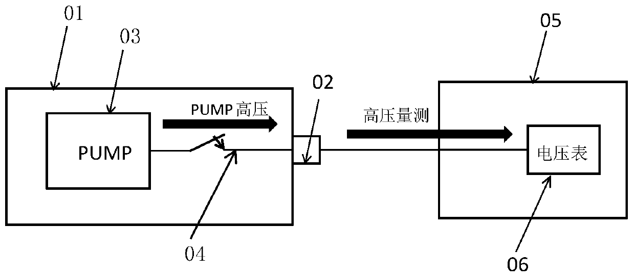
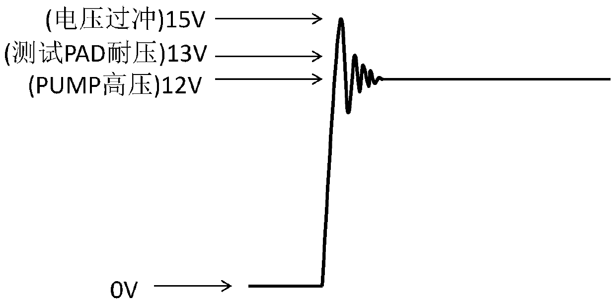
[0035] Step 1. Apply a first voltage on the pad 02, and then turn on the switch 04; since the pad is at zero voltage before the test, if the output voltage of the charge pump 03 is directly received, the output voltage Generally, it is a high voltage. Since the bonding pad 02 has a certain withstand voltage capability, the high voltage will cause voltage overshoot to it, causing it to be permanently damaged and unable to be reused, reducing the yield rate of the test chip. Therefore, before the charge pump turns on the output voltage, a certain voltage is firstly applied to the pad, and in this embodiment, the applied first voltage is a low voltage. The low voltage is lower than the output voltage of the charge pump. Preferably, the first voltage applied to the pad is 5V. Preferably, a voltage source 07 is provided inside the testing ma...

Embodiment 2

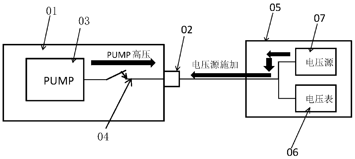
[0043] The present embodiment provides a kind of test method that prevents high pressure from burning welding pad, such as Figure 3a as shown, Figure 3a A schematic diagram showing the application of voltages to pads in the present invention.

[0044] Firstly, a chip under test 01 and a testing machine 05 are provided, and the chip under test is preferably an embedded FLASH chip in this embodiment. The chip under test 01 is connected to the testing machine 05 .

[0045] Such as Figure 3a As shown, the chip under test 01 has a charge pump 03 and a welding pad 02, and a switch 04 is connected between the charge pump 03 and the welding pad 02, and the welding pad 02 is connected to the testing machine 05. Embodiments Preferably, the switch 04 on the chip under test 01 is controlled by a switch circuit, the switch circuit is activated, the switch 04 is turned on, and the output voltage of the charge pump 03 is transmitted to the pad 02 Since the welding pad 02 is connected ...


PUM


Abstract

The invention provides a test method for preventing high-voltage PAD burning, and the method comprises the steps: providing a tested chip and a test machine, enabling the tested chip to be provided with a charge pump and a welding pad, enabling the charge pump and the welding pad to be connected through a switch, enabling the welding pad to be connected with the test machine, applying a first voltage to the welding pad, and then opening the switch;starting the charge pump to output a second voltage; increasing the first voltage to a third voltage, wherein the third voltage is smaller than thesecond voltage; cutting off the third voltage on the welding pad to enable the voltage on the welding pad to rise from the third voltage to the second voltage; and testing the second voltage output bythe charge pump on the welding pad by using a testing machine. According to the invention, the voltage is applied to the welding pad in advance, and then slowly rises to reduce the voltage overshootgenerated during the high-voltage starting output of the charge pump, so that the risk that the test welding pad is damaged by the high-voltage overshoot is avoided, and the yield is improved.

Description

technical field [0001] The invention relates to a chip testing method, in particular to a testing method for preventing high-pressure burning pads. Background technique [0002] In the test of the embedded FLASH chip, it is necessary to adjust (TRIMMING) the charge pump (PUMP) voltage on the FLASH chip, so that the PUMP voltage of all tested chips can be kept within the specification range. Such as figure 1 as shown, figure 1 Shown is a schematic diagram of an on-chip charge pump voltage test in the prior art. The chip under test 01 is connected to the testing machine 05, and the chip under test 01 has a charge pump 03 and a pad 02, and a switch 04 is connected between the charge pump 03 and the pad 02, and the pad 02 is connected to the pad 02. The testing machine 05 is connected through a voltmeter 06. [0003] The charge pump (PUMP) voltage is generally relatively high, between 8V and 12V. When adjusting (TRIMMING), it is necessary to connect the charge pump (PUMP) to...

Claims


Application Information

Patent Timeline
IPC IPC(8): G11C29/56
Inventor 朱渊源
Owner SHANGHAI HUAHONG GRACE SEMICON MFG CORP
Why Eureka
Try Eureka