

Method for preparing graphene by combining germanium concentration and ion implantation technology
A technology of ion implantation and graphene, which is applied in the direction of graphene, semiconductor/solid-state device manufacturing, electrical components, etc., can solve problems such as damage and fracture, influence of device preparation, impurity defects and pollution, so as to reduce loss and avoid secondary transfer Effect
Patent Information
- Authority / Receiving Office
- CN · China
- Patent Type
- Applications(China)
- Current Assignee / Owner
- Publication Date
- 2019-06-14
- Estimated Expiration
- Not applicable · inactive patent
Smart Images
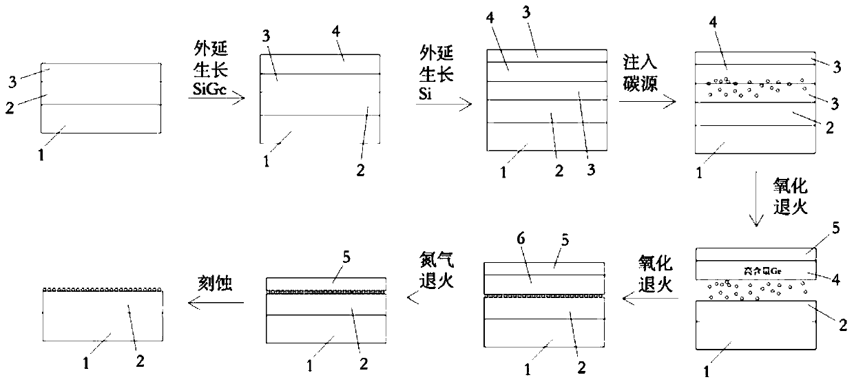
Figure 1 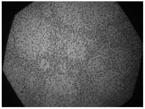
Figure 2 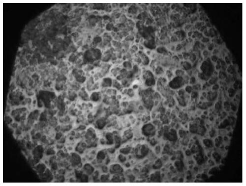
Figure 3
Abstract
Description
Technical field
[0001] The invention relates to a method for preparing graphene by combining germanium concentration and ion implantation technology, belonging to the field of graphene preparation.
Background technique
[0002] In 2004, Andre Geim and Konstantin Novoselov, physicists at the University of Manchester in the United Kingdom, successfully separated graphene from graphite by using mechanical exfoliation, and confirmed that it can exist alone. As a result, they jointly won the 2010 Nobel Prize in Physics. Since the discovery of graphene, with its unique physical, chemical, electrical and many other properties and wide application prospects, it has set off a research frenzy in the fields of academic research and industry.
[0003] Due to the specific physical characteristics of graphene such as zero band gap and lack of single crystals, especially the incompatibility between the current graphene preparation technology and mature semiconductor technology, graphe...
Examples
Embodiment 1
[0030] see Figure 1-2 , what this embodiment provides is a kind of method that combines germanium concentration and ion implantation technology to prepare graphene, comprises the following steps:
[0031] Step ①: Provide SOI substrate, which includes Si substrate layer 1 (Si sub, 30nm), SiO 2 Substrate layer 2 (300nm) and Si layer 3 (30nm), SiGe composite layer 4 (75nm) is chemically vapor deposited on the surface of Si layer 3, SiGe composite layer 4 is composed of Ge simple substance and Si simple substance, wherein Ge simple substance accounts for SiGe composite layer 4 30% of the total mass is affected by the simple substance Si, and the melting point of the simple substance Ge in the SiGe composite layer 4 is increased;
[0032] Step ②: use chemical vapor deposition to epitaxially grow a layer of Si layer 3 (4nm) on the surface of the SiGe composite layer 4 away from the SOI substrate again, so that the SiGe composite layer 4 is locked between the two Si layers 3, so as...
Embodiment 2
[0048] see image 3 , The difference between this embodiment and Embodiment 1 is that in step ①, the thickness of the Si layer of the SOI substrate is 100 nm, and it can be seen that although graphene is grown, it is very uneven. The main reason may be that during the annealing process, the SiGe composite layer and SiO 2 The increase in the distance between the substrate layers increases the movement distance of the carbon ions in the middle of the SiGe composite layer to the edge of the SiGe composite layer, so the corresponding carbon ions move to the SiO 2 After the substrate layer is more uneven, the growth of graphene is more uneven. At the same time, due to the early SiO 2 The substrate layer acts as a barrier to carbon ions, so carbon ions will be unevenly distributed in the Si layer before annealing and heating, resulting in differences in the growth base points of graphene at different positions.
Embodiment 3
[0050] see Figure 4 , The difference between this embodiment and Embodiment 1 is that in step ①, Ge simple substance accounts for 50% of the total mass of the SiGe composite layer. It can be seen that graphene is still growing, and the growth rate of graphene has been greatly improved due to the increase in the content of Ge element, but because Ge element will be vaporized during the annealing process in nitrogen environment, but due to the SiO 2 The shielding effect of the layer, the vaporization position is more intense at the edge of the Ge layer, the greater the content of Ge element, the greater the difference in the growth rate and degree of the corresponding graphene between the edge and the center.