soi LIGBT device with diode-clamped carrier storage layer

A carrier storage and diode clamping technology, applied in semiconductor devices, electrical components, circuits, etc., to achieve the effects of excellent short-circuit resistance, reduced conduction voltage drop, and low saturation current density

Active Publication Date: 2020-08-18
UNIV OF ELECTRONICS SCI & TECH OF CHINA
View PDF4 Cites 0 Cited by
  • Summary
  • Abstract
  • Description
  • Claims
  • Application Information

AI Technical Summary

Problems solved by technology

[0005] However, in prior art LIGBT devices with a carrier storage layer, as the carrier storage layer concentration (Carrier-Stored Layer Concentration: N cs ) increases, the breakdown voltage (BreakdownVoltage: BV) of the device will decrease accordingly

Method used


Image

  • soi LIGBT device with diode-clamped carrier storage layer
  • soi LIGBT device with diode-clamped carrier storage layer
  • soi LIGBT device with diode-clamped carrier storage layer

Examples


Embodiment 1

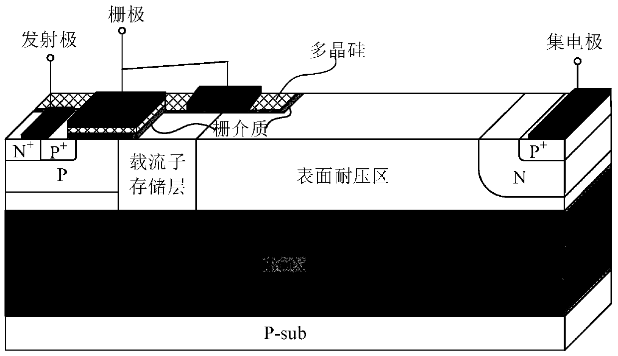
[0036] An embodiment of the present invention provides an SOI LIGBT device with two diode clamps, such as Figure 2 ~ Figure 3 Commonly shown, it includes a semiconductor substrate 1 , a buried oxide layer region 2 on the semiconductor substrate 1 , and a semiconductor layer (SOI layer) on the buried oxide layer region 2 . The semiconductor layer includes a P-type semiconductor base region 3, a gate region, an N-type carrier storage region 6, a surface withstand voltage region 7, a P-type electric field shielding region 13, an N-type semiconductor buffer region 15, and a P-type collector region 16, The P-type semiconductor base region 3 and the gate region are located on one side of the semiconductor layer, the N-type semiconductor buffer zone 15 is located on the other side of the semiconductor layer, and the N-type carrier storage region 6 is located next to the P-type semiconductor base region 3, and the P-type electric field shielding The region 13 is located next to the g...

Embodiment 2

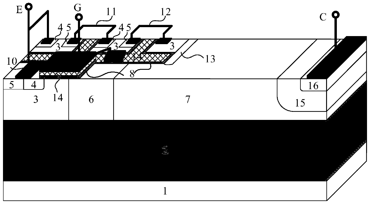
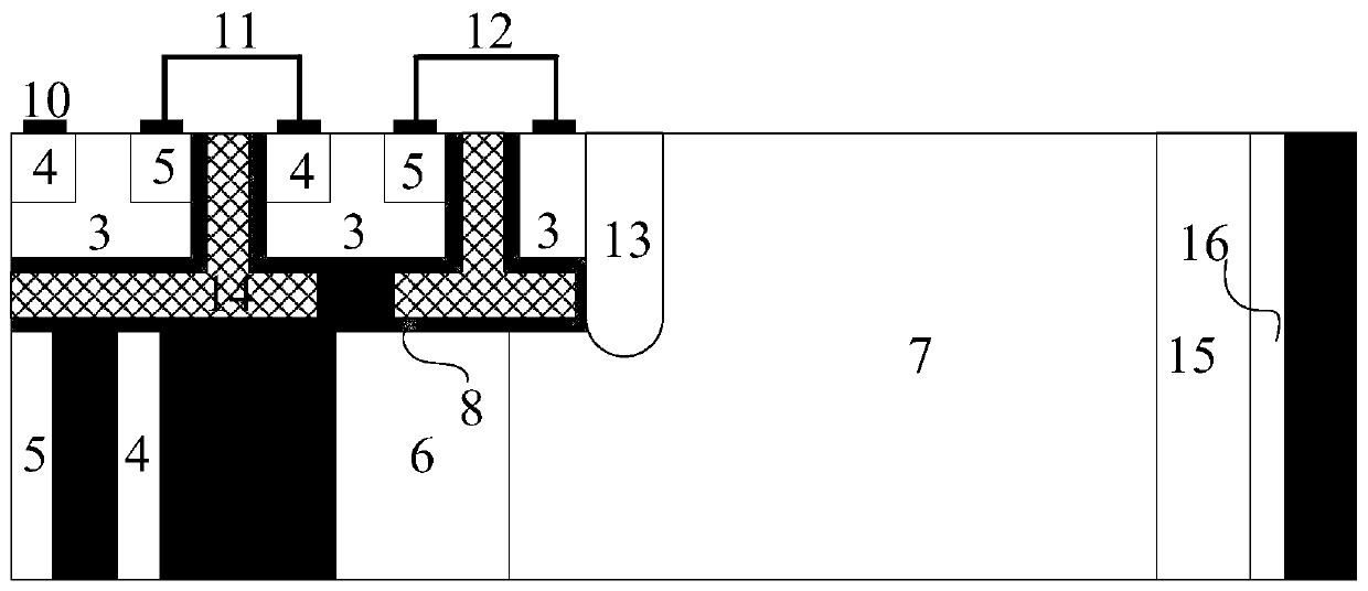
[0047] An embodiment of the present invention provides an SOI LIGBT device with three diode clamps, such as Figure 4 ~ Figure 5 Commonly shown, it includes a semiconductor substrate 1 , a buried oxide layer region 2 on the semiconductor substrate 1 , and a semiconductor layer (SOI layer) on the buried oxide layer region 2 . The semiconductor layer includes a P-type semiconductor base region 3, a gate region, an N-type carrier storage region 6, a surface withstand voltage region 7, a P-type electric field shielding region 13, an N-type semiconductor buffer region 15, and a P-type collector region 16, The P-type semiconductor base region 3 and the gate region are located on one side of the semiconductor layer, the N-type semiconductor buffer zone 15 is located on the other side of the semiconductor layer, and the N-type carrier storage region 6 is located next to the P-type semiconductor base region 3, and the P-type electric field shielding The region 13 is located beside the ...


PUM


Abstract

The invention discloses an SOI LIGBT device with a diode-clamped carrier storage layer. By dividing the P-type semiconductor base region into multiple regions and introducing two or three series diodes in different regions, the device can be used in reverse When the potential of the P-type electric field shielding area rises to the conduction voltage drop of two or three diodes, the diode is turned on, and the potential of the P-type electric field shielding area is clamped to two or three diodes. The voltage drop is close, so the potential of the N-type carrier storage region is well shielded by the P-type electric field shielding region at a very low value, and the withstand voltage of the device will mainly be the reverse of the P-type electric field shielding region and the surface withstand voltage region. The biased diode bears, thus completely breaking the contradictory relationship between the breakdown voltage and the concentration of the N-type carrier layer.

Description

technical field [0001] The invention belongs to the technical field of power semiconductor devices, and in particular relates to the design of an SOI LIGBT device with a diode-clamped carrier storage layer. Background technique [0002] The miniaturization and integration of power electronic systems is an important research direction of power semiconductor devices. Smart Power Integrated Circuit (SPIC) or High Voltage Integrated Circuit (HVIC) integrates low-voltage circuits such as protection, control, detection, and drive and high-voltage power devices on the same chip, which not only reduces the size of the system volume, but also improves system reliability. At the same time, in higher frequency working occasions, due to the reduction of system lead inductance, the requirements for buffer and protection circuits can be significantly reduced. [0003] Lateral Insulated-Gate Bipolar Transistor (LIGBT) is one of the important power devices of SPIC or HVIC, and LIGBT based...

Claims


Application Information

Patent Timeline
Patent Type & Authority Patents(China)
IPC IPC(8): H01L29/739H01L29/06
Inventor 易波蔺佳杨瑞丰彭一峰
Owner UNIV OF ELECTRONICS SCI & TECH OF CHINA
Why Eureka
Try Eureka