Deep ultraviolet light emitting diode package

A technology for light-emitting diodes and packaging structures, applied in electrical components, circuits, semiconductor devices, etc., can solve problems such as package breakage and performance degradation of bonding materials

Active Publication Date: 2019-06-14
EPITOP PHOTOELECTRIC TECH
View PDF6 Cites 11 Cited by
  • Summary
  • Abstract
  • Description
  • Claims
  • Application Information

AI Technical Summary

Problems solved by technology

[0005] The present invention provides a deep ultraviolet light-emitting diode packaging structure. By opening a groove on an insulating substrate and then bonding a light-transmitting component in the groove, it solves the problem that the bonding

Method used


Image

  • Deep ultraviolet light emitting diode package
  • Deep ultraviolet light emitting diode package
  • Deep ultraviolet light emitting diode package

Examples


Embodiment 1

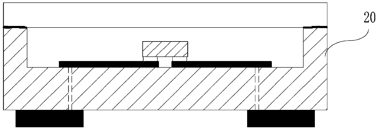
[0027] In recent years, deep ultraviolet light-emitting diodes have broad application prospects in the fields of sterilization and disinfection, polymer curing, biochemical detection, non-line-of-sight communication and special lighting. Compared with traditional ultraviolet light source mercury lamps, they are environmentally friendly, compact and portable, low power consumption, Low voltage and many other well-known advantages, the packaging structure of deep ultraviolet light-emitting diodes generally adopts an integrally formed insulating substrate and a support structure 20 composed of dams to place deep ultraviolet light-emitting diode chips, such as figure 1 As shown, in this packaging structure, the optical lens and the top of the dam are bonded together by an adhesive material or a welding material, so that a closed space is formed between the support structure 20 and the optical lens. In the current packaging structure, some inorganic packaging is used. This is becaus...

Embodiment 2

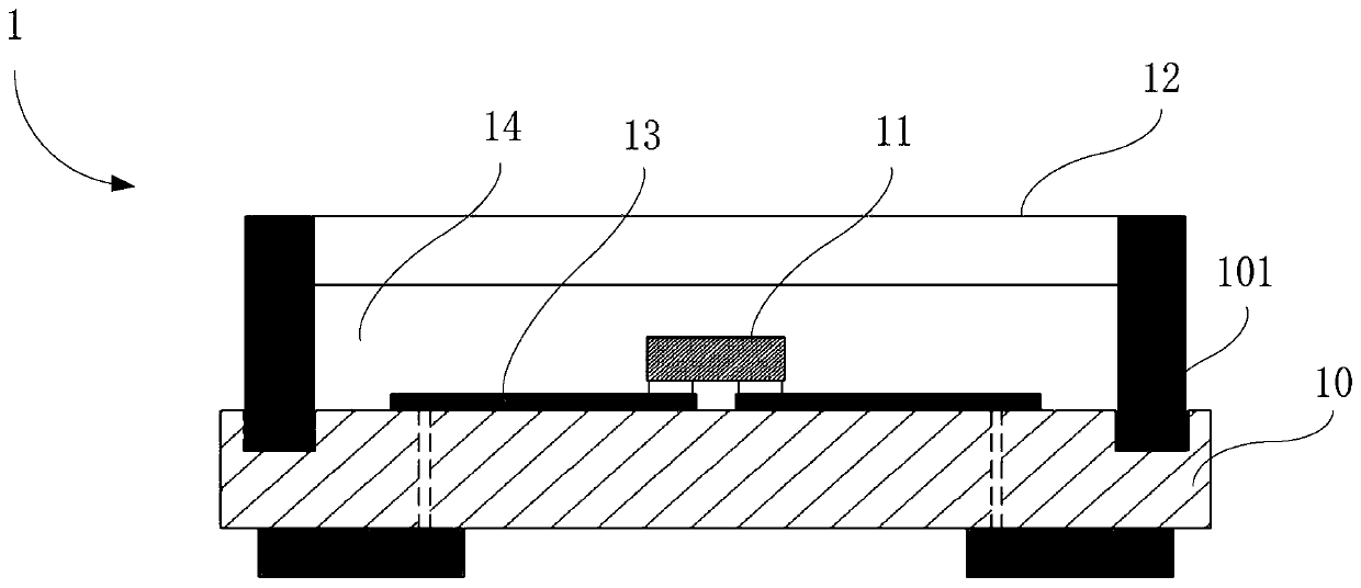
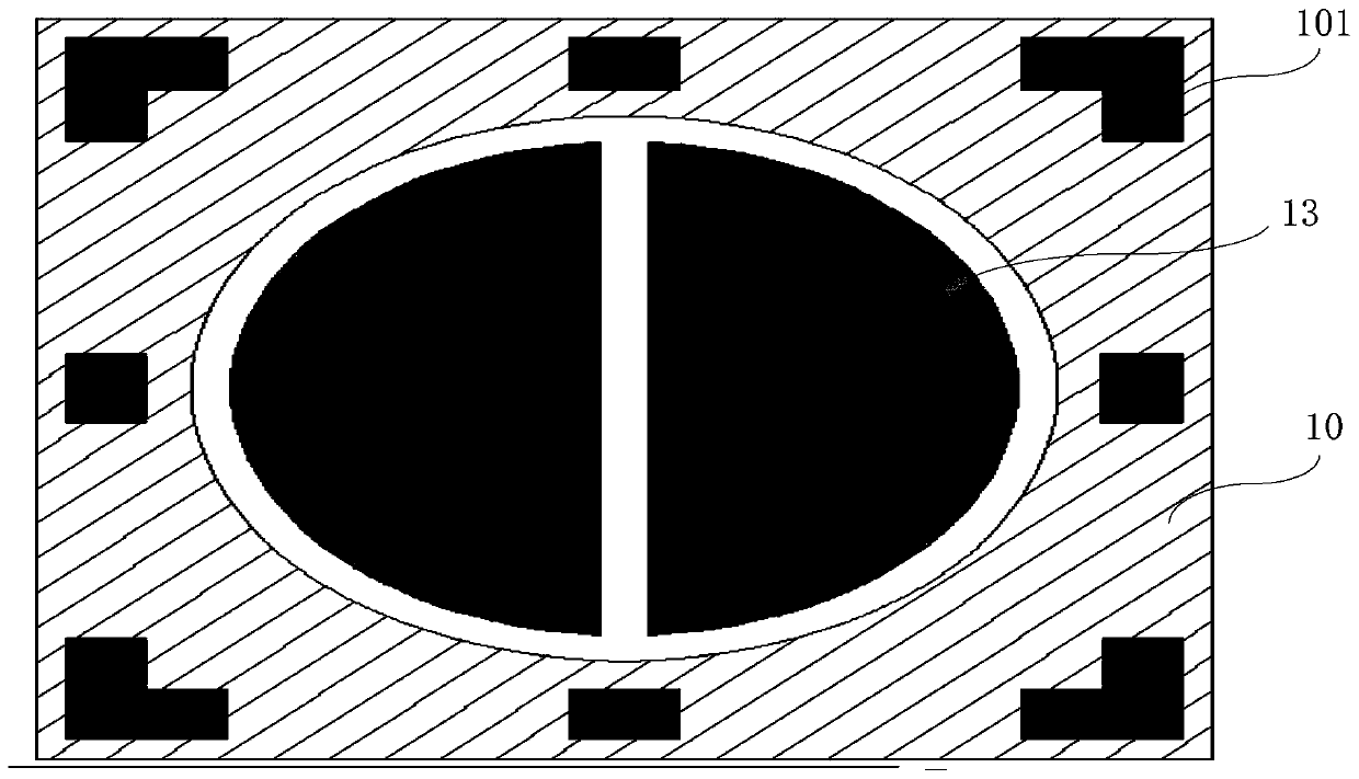
[0042] This embodiment provides a deep ultraviolet light emitting diode packaging structure 1, such as Figure 6 As shown, it includes: an insulating substrate 10, a light-emitting diode chip 11, a welding pad 13, and a light-transmitting component 12, wherein an inwardly recessed groove 101 is opened on the edge of the insulating substrate 10, and the light-transmitting component 12 is covered on the insulating substrate. 10 and the bottom end of the light-transmitting component 12 is bonded in the groove 101, the light-transmitting component 12 and the insulating substrate 10 jointly enclose a closed accommodation space 14, and the light-emitting diode chip 11 and the welding pad 13 are located in the accommodation space 14 , the welding pad 13 is arranged on the insulating substrate 10, and the light-emitting diode chip 11 is electrically connected to the welding pad 13. In the working state, the deep ultraviolet light emitted by the light-emitting diode chip 11 will fill th...

Embodiment 3

[0047] This embodiment provides a deep ultraviolet light emitting diode packaging structure 1, such as Figure 7 As shown, it includes: an insulating substrate 10, a light-emitting diode chip 11, a welding pad 13, and a light-transmitting component 12, wherein an inwardly recessed groove 101 is opened on the edge of the insulating substrate 10, and the light-transmitting component 12 is covered on the insulating substrate. 10 and the bottom end of the light-transmitting component 12 is bonded in the groove 101, the light-transmitting component 12 and the insulating substrate 10 jointly enclose a closed accommodation space 14, and the light-emitting diode chip 11 and the welding pad 13 are located in the accommodation space 14 , the welding pad 13 is arranged on the insulating substrate 10, and the light-emitting diode chip 11 is electrically connected to the welding pad 13. In the working state, the deep ultraviolet light emitted by the light-emitting diode chip 11 will fill th...


PUM


Abstract

The invention provides a deep ultraviolet light emitting diode package structure. The deep ultraviolet light emitting diode package structure comprises an insulating substrate, a light emitting diodechip, a soldering pad and a light transmissive component; wherein a groove is formed on the edge of the insulating substrate; the bottom end of the light transmissive component is bonded in the groove, and the light transmissive component and the insulating substrate together form a closed accommodating space; the light emitting diode chip and the soldering pad are located in the accommodating space; the soldering pad is disposed on the insulating substrate; and the light emitting diode chip is electrically connected to the soldering pad. The package structure provided by the invention binds the light transmissive component to the groove formed on the insulating substrate, so that the bonding material is not directly exposed to the deep ultraviolet light; therefore, the performance degradation of the bonding material is avoided, the sealing performance of the packaging structure is ensured, the shear resistance of the packaging structure is improved, and the service life of the packaging structure is prolonged.

Description

technical field [0001] The invention relates to the field of semiconductor device manufacturing, in particular to a deep ultraviolet light emitting diode package. Background technique [0002] Deep ultraviolet light-emitting diodes (UV LEDs) based on III-nitride materials have broad applications in fields such as sterilization and disinfection, polymer curing, biochemical detection, non-line-of-sight communication, and special lighting. Compared with mercury lamps, deep ultraviolet light-emitting diodes have many advantages such as environmental protection, compactness and portability, low power consumption, and low voltage. Therefore, they have received more and more attention and applications in recent years. [0003] At present, in the tube packaging structure of deep ultraviolet light-emitting diodes, the support structure in which the insulating substrate and the dam are integrally formed is generally used to place the light-emitting deep ultraviolet diode chip, and the...

Claims


Application Information

Patent Timeline
IPC IPC(8): H01L33/48H01L33/58
Inventor 康建姚禹郑远志陈向东梁旭东
Owner EPITOP PHOTOELECTRIC TECH
Why Eureka
Try Eureka