Full-inorganic ultraviolet LED wafer-level package method

A wafer-level packaging and LED packaging technology, which is applied in the direction of electrical components, circuits, semiconductor devices, etc., can solve the problems of modern packaging requirements for hard-to-ultraviolet LEDs, high packaging costs, and low process integration, and meet long-term reliability requirements , reduce packaging cost, improve the effect of packaging integration

Active Publication Date: 2019-06-14
武汉高星紫外光电科技有限公司
View PDF5 Cites 4 Cited by
  • Summary
  • Abstract
  • Description
  • Claims
  • Application Information

AI Technical Summary

Problems solved by technology

However, the existing UV LED packaging process is still to implement SMT, wire bonding, glass cover bonding and other processes on the UV LED chip respectively. There are many process steps, low process integration and high packaging cost, so it is difficult to meet the modernization requirements of UV LEDs. Packaging requirements

Method used


Image

  • Full-inorganic ultraviolet LED wafer-level package method
  • Full-inorganic ultraviolet LED wafer-level package method

Examples


Embodiment 1

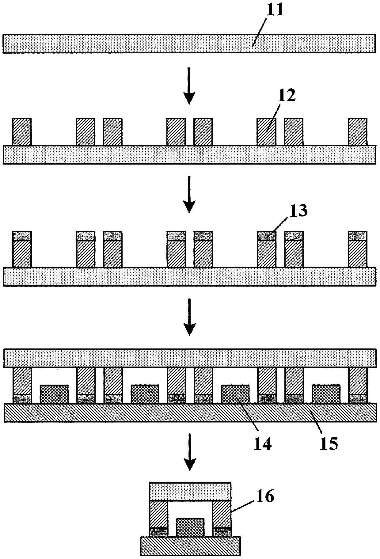
[0031] See figure 1 , This embodiment 1 provides an all-inorganic UV LED wafer-level packaging method, which as an example may include the following steps:

[0032] Step 1. First prepare glass slurry, mix glass powder, ceramic powder and binder, and stir them thoroughly. The components are set as follows: Low melting point borosilicate glass is selected for glass powder and its content is the total weight of the slurry 70%, the ceramic powder chooses alumina material and its content is 20% of the total weight of the slurry, and the glass powder and ceramic powder have a particle size of 5-10μm, and the binder is a mixture of ethyl cellulose and terpineol. , And the mixing amount is respectively 2% and 8% of the total weight of the slurry; then a 0.5mm thick quartz glass sheet is selected as the glass cover 11, and multiple round glasses are printed on the glass cover 11 by 3D printing technology Then place the glass cover 11 in a high-temperature furnace, first dry at 250°C for 2...

Embodiment 2

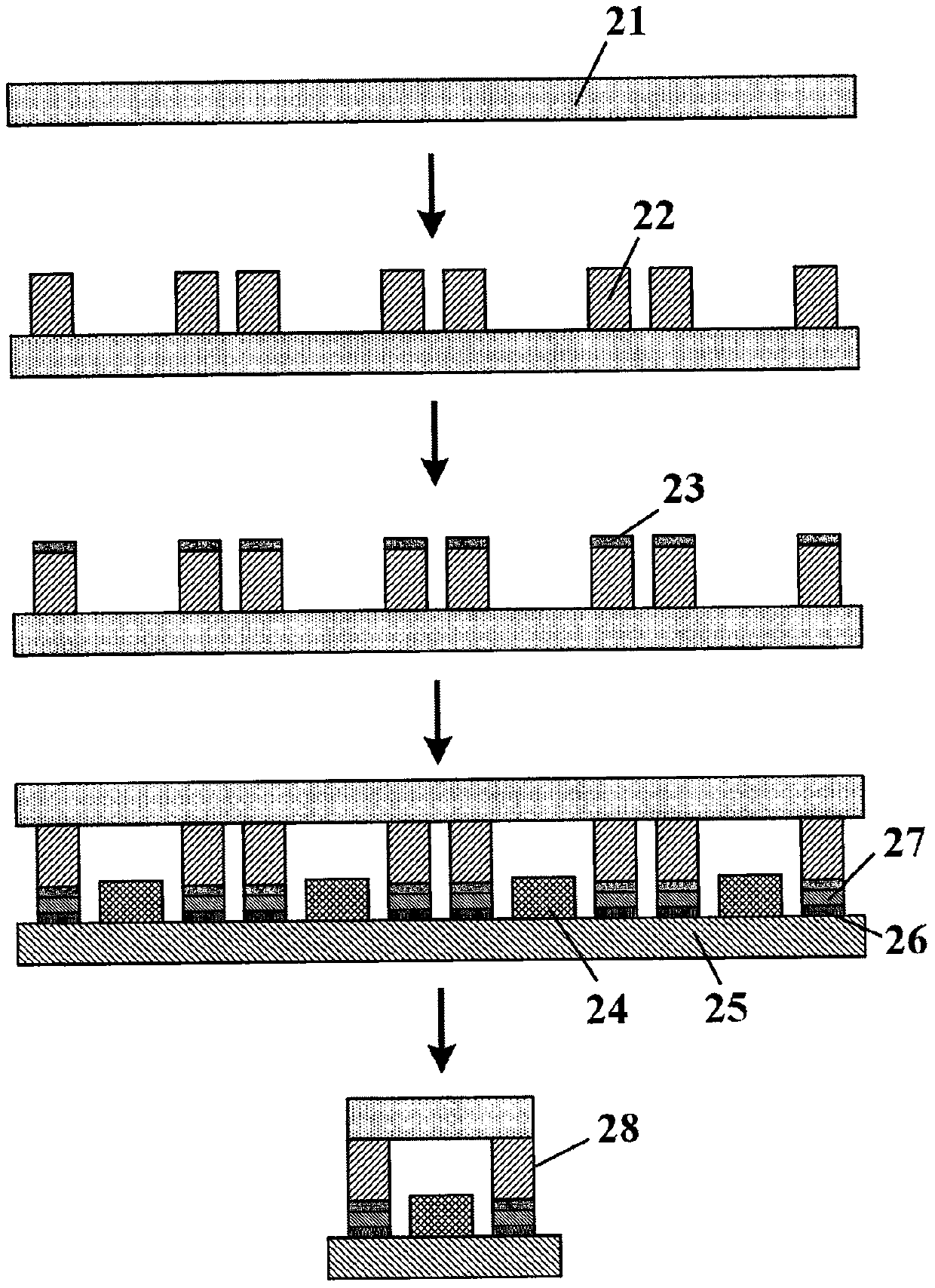
[0038] See figure 2 , This embodiment 2 provides a method for all-inorganic UV LED wafer-level packaging, which as an example may include the following steps:

[0039] Step 1. First prepare glass slurry, mix glass powder, ceramic powder and binder, and stir them thoroughly. The components are set as follows: Low melting point borosilicate glass is selected for glass powder and its content is the total weight of the slurry 65%, ceramic powder chooses alumina material and its content is 20% of the total weight of the slurry, and the particle size of glass powder and ceramic powder is 5-10μm, and the binder is selected as a mixture of ethyl cellulose and terpineol , And its content is respectively 5% and 10% of the total weight of the paste; then a 0.5mm thick quartz glass sheet is selected as the glass cover 21, and a square glass paste is printed on the glass cover 21 by multiple screen printing The material ring is dried at 200°C for 30 minutes after each printing, and then the...


PUM


Abstract

The invention belongs to the technical field of semiconductor manufacturing, and discloses a full-inorganic ultraviolet LED wafer-level package method. The full-inorganic ultraviolet LED wafer-level package method comprises the steps of firstly, forming a plurality of glass paste rings on a glass cover plate by a printing or 3D printing technology, and obtaining a plurality of glass cavity structures by low-temperature sintering; secondly, surface-mounting a plurality of ultraviolet LED chips onto a cooling substrate; thirdly, achieving reliable bonding of the glass cavities in the glass coverplate and the cooling substrate by inorganic paste or a metal welding material; and finally, cutting to obtain a full-inorganic ultraviolet LED package product. The invention also discloses a corresponding ultraviolet LED package structure. By the full-inorganic ultraviolet LED wafer-level package method, the problems of ultraviolet aging and failure of an organic package material are effectivelyprevented, the long-term reliability of an ultraviolet LED device is improved, the ultraviolet LED package integration is improved, and the package cost is reduced.

Description

Technical field [0001] The invention belongs to the related field of semiconductor manufacturing technology, and more specifically, relates to a wafer-level packaging method for all-inorganic ultraviolet LEDs. Background technique [0002] Compared with traditional ultraviolet light sources such as mercury lamps, ultraviolet LEDs have many advantages such as mercury-free environmental protection, low power consumption, and controllable wavelength. Ultraviolet LEDs can be divided into light ultraviolet LEDs (>300nm) and deep ultraviolet LEDs (≤300nm) according to their different emission wavelengths. At present, light ultraviolet LEDs have been widely used in ink printing, resin curing, inspection and identification and other fields. With the development of ultraviolet LED technology, deep ultraviolet LEDs will have a broad range of fields such as sterilization and disinfection, water purification, medical beauty, and biochemical testing. Application prospects. [0003] LED pac...

Claims


Application Information

Patent Timeline
Patent Type & Authority Applications(China)
IPC IPC(8): H01L33/48H01L33/56
Inventor 彭洋柳星星陈明祥
Owner 武汉高星紫外光电科技有限公司
Why Eureka
Try Eureka