
Self-repairing method for phased-array antenna microsystem integrated packaging structure

A phased array antenna and integrated packaging technology, which is applied in the direction of antenna support/mounting device, antenna, antenna array, etc., can solve the problems of deterioration of electrical performance of devices, incomplete melting of solder balls, shortening service life of devices, etc., and meet the requirements of Long-term reliability requirements, improving electrical interconnection reliability, and increasing the effect of service life

Active Publication Date: 2022-02-15
10TH RES INST OF CETC
View PDF14 Cites 0 Cited by
  • Summary
  • Abstract
  • Description
  • Claims
  • Application Information

AI Technical Summary

Problems solved by technology

The main defects of solder joints are: void, desoldering (open circuit), bridging (short circuit), internal cracks in solder balls, disturbance of solder joints, cold soldering, incomplete melting of solder balls, displacement (solder balls are not aligned with PCB pads), Solder beads, etc.
Nevertheless, in practical applications, friction, collision, bending, etc. will inevitably bring mechanical damage such as scratches, creases, and cracks to flexible electronic devices, and these damages may cause the electrical performance of the device to deteriorate or even fail, thereby shortening the life of the flexible electronic device. Device life
For example, for a plate capacitor with a carbon nanotube conductive network as an electrode, when a crack is generated on the electrode, the conductivity of the electrode decreases due to the blockage of the carbon nanotube conductive network, resulting in a large decrease in the capacitance of the device; For piezoresistive sensors that use materials or conductive materials / polymer composites as sensitive materials, when a crack occurs in the material, the resistance of the material increases greatly, and it cannot be used as a sensitive material for the sensor; for wearable electronic devices, tiny cracks It will continue to expand during human movement, and even cause device breakage and functional failure

Method used


Image

  • Self-repairing method for phased-array antenna microsystem integrated packaging structure

Examples


Embodiment Construction

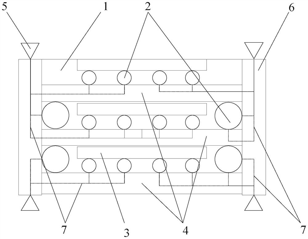
[0017] refer to figure 1 . According to the present invention, arrays are made on the top and bottom of the packaging substrate 4 that encapsulates the active components 3, and the solder balls are used as the I / O terminals of the circuit to connect with the printed circuit board PCB, through the interconnection solder joints 2 network solder ball arrays and Embedded wafer-level ball grid array eWLB realizes single-chip wafer-level packaging including baseband, processor, memory, power management, and radio frequency transceivers, through the layer-by-layer interconnection between each redistribution layer and the packaging substrate 4 At the same time, the electrical signal transmission between the packaging substrate 4 is also realized through the interconnection solder joints 2, forming a microsystem package 1 for packaging microsystem integrated components; a repairable package carrier 6 is arranged at both ends of the microsystem package 1, and can be placed on the two en...


PUM


Abstract

A self-repairing method of a phased array antenna microsystem integrated packaging structure disclosed by the invention has high packaging reliability and does not damage pins. According to the technical scheme, arrays are manufactured on the upper face and at the bottom of a packaging substrate where active components are packaged, wafer-level packaging of all the components is achieved through interconnection of welding spot network welding ball arrays and embedded wafer-level ball grid arrays, electric signal transmission between the packaging substrates is achieved through layer-by-layer interconnection to form a microsystem packaging body for packaging a microsystem integrated component; repairable packaging carriers are arranged at the two ends of the microsystem packaging body, capillary filling pipelines communicated with channels of all layers of packaging substrates are manufactured on the repairable packaging carriers, and when the interconnection welding spots of the microsystem integrated assembly are in a defect in the service process, liquid metal supplements the interconnection welding spots through a liquid metal self-filling interface arranged on the repairable packaging carriers, and the liquid metal is molded after injection and is integrated with the welding spots.

Description

technical field [0001] The invention relates to a self-repairing system packaging method that can be filled with liquid metal, in particular to a self-repairing method for a phased array antenna microsystem integrated packaging structure. Background technique [0002] Microsystem integration products can improve their reliability and adaptability to special environments such as radiation resistance, and are one of the technical approaches to focus on oceans, space, and electromagnetics. Microelectronic packages and chips (Chip or die) are combined into a microelectronic device (Device) through packaging technology (Packaging), usually packaged to provide electrical pathways, heat dissipation pathways, mechanical support, environmental protection, etc. for the chip (or die), Therefore, microelectronic packaging is one of the two basic components of microelectronic devices, and many reliability performances of devices are determined by the performance of packaging. Microelect...

Claims


Application Information

Patent Timeline
Patent Type & Authority Applications(China)
IPC IPC(8): H01Q21/00H01L23/66H01Q1/22H01Q1/38
CPCH01Q21/00H01Q1/2283H01Q1/38H01L23/66H01L2223/6677
Inventor 海洋鲁聪
Owner 10TH RES INST OF CETC
Learn More