A Plasma Cutting Process for Realizing Ultra-Narrow Cutting Road

An ultra-narrow slit and plasma technology, which is applied in the direction of plasma welding equipment, welding/welding/cutting items, manufacturing tools, etc., can solve problems such as product strength decline, product chip rupture, and difficulty in ultra-narrow slit cutting.

Active Publication Date: 2021-11-02
RF360 TECH (WUXI) CO LTD
View PDF13 Cites 0 Cited by
  • Summary
  • Abstract
  • Description
  • Claims
  • Application Information

AI Technical Summary

Problems solved by technology

[0003] In view of the fact that the existing cutting process in the prior art is difficult to achieve ultra-narrow kerf cutting, especially for kerf cutting with a width less than 30 μm, and it is easy to cause a decrease in product strength, resulting in the problem that product chips are prone to cracks in subsequent production. The invention provides a process for plasma cutting to realize ultra-narrow slits, which can realize the cutting of ultra-narrow slits on semiconductor wafers, effectively maintain product strength, and avoid the problem of product chip breakage in subsequent production

Method used


Image

  • A Plasma Cutting Process for Realizing Ultra-Narrow Cutting Road
  • A Plasma Cutting Process for Realizing Ultra-Narrow Cutting Road
  • A Plasma Cutting Process for Realizing Ultra-Narrow Cutting Road

Examples


Embodiment 1

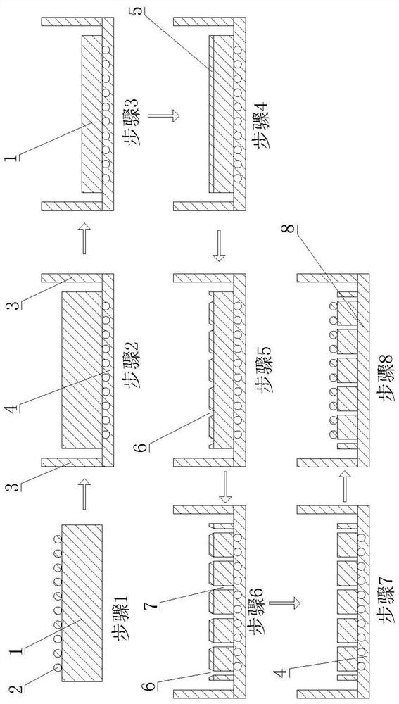
[0026] Such as figure 1 Shown, embodiment one: a kind of technology that plasma cutting realizes ultra-narrow cutting line, it comprises the following process steps:

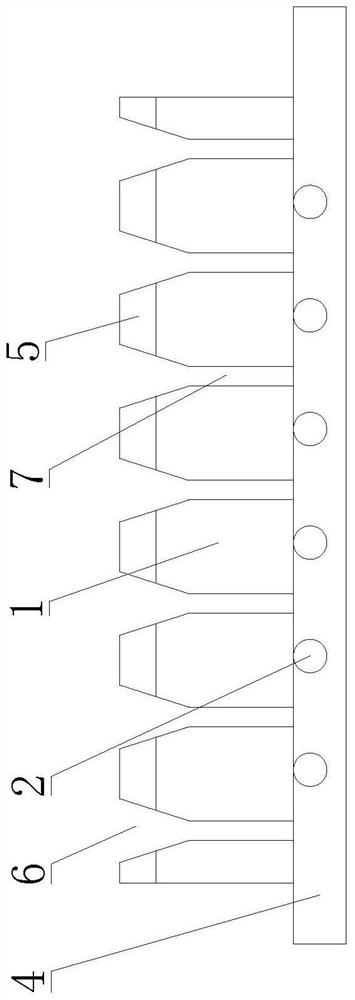
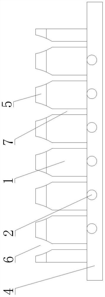
[0027] Step 1: Do ball planting 2 on the front side of the semiconductor wafer 1 by solder paste printing and reflow soldering process. The solder paste printing is to print the solder paste on the front side of the semiconductor wafer 1 by using the movement of the solder paste scraper of the solder paste printing machine. The angle of the paste scraper is 30 degrees, and the movement speed is 5 mm / s; then, the solder paste is melted and soldered by the reflow process to form solder balls 2, and the peak temperature of the reflow soldering is 213 degrees;

[0028] Step 2: Attach the metal ring 3 whose size is suitable for the semiconductor wafer 1 on the BG-UV film 4 by roller pressure, then turn over the semiconductor wafer 1 processed in step 1, and make it face down by roller pressure Mounted on the inner s...

Embodiment 2

[0036] Embodiment 2: A process for realizing ultra-narrow cutting lines by plasma cutting, which includes the following process steps:

[0037] Step 1: Do ball planting 2 on the front side of the semiconductor wafer 1 by solder paste printing and reflow soldering process. The solder paste printing is to print the solder paste on the front side of the semiconductor wafer 1 by using the movement of the solder paste scraper of the solder paste printing machine. The angle of the paste scraper is 60 degrees, and the movement speed is 60 mm / s; then the solder paste is melted and soldered through the reflow soldering process, and the peak temperature of the reflow soldering is 213 degrees;

[0038]Step 2: Attach the metal ring 3 whose size is suitable for the semiconductor wafer 1 on the BG-UV film 4 by roller pressure, then turn over the semiconductor wafer 1 processed in step 1, and make it face down by roller pressure Mounted on the inner side of the metal ring 3, all the balls 2 ...

Embodiment 3

[0046] Embodiment 3: A process for realizing ultra-narrow cutting lines by plasma cutting, which includes the following process steps:

[0047] Step 1: Do ball planting 2 on the front side of the semiconductor wafer 1 by solder paste printing and reflow soldering process. The solder paste printing is to print the solder paste on the front side of the semiconductor wafer 1 by using the movement of the solder paste scraper of the solder paste printing machine. The angle of the paste scraper is 45 degrees, and the movement speed is 27.5 mm / s; then the solder paste is melted and soldered through the reflow process, and the peak temperature of the reflow soldering is 213 degrees;

[0048] Step 2: Attach the metal ring 3 whose size is suitable for the semiconductor wafer 1 on the BG-UV film 4 by roller pressure, then turn over the semiconductor wafer 1 processed in step 1, and make it face down by roller pressure Mounted on the inner side of the metal ring 3, the ball planting 2 is ...


PUM


Abstract

A process for plasma cutting to realize ultra-narrow slits, which can realize the cutting of ultra-narrow slits on semiconductor wafers, can effectively maintain product strength, and avoid the problem of product chip rupture in subsequent production, which includes the following process steps : Step 1, do ball planting on the front side of the semiconductor wafer, step 2: attach the metal ring whose size is suitable for the semiconductor wafer to the BG‑UV film, and then flip the semiconductor wafer and attach it to the inner side of the metal ring , step 3: use semiconductor wafer grinding equipment to reduce the thickness of the semiconductor wafer, step 4: apply protective glue to the back of the semiconductor wafer, step 5: groove the protective glue on the back of the semiconductor wafer, Step 6: Corresponding to the grooved position of the protective glue, use a plasma cutting machine to cut the ultra-narrow slit on the back of the semiconductor wafer. Step 7: Clean the semiconductor wafer with the protective glue. Step 8: Cut the semiconductor wafer Pour round onto DC‑UV film.

Description

technical field [0001] The invention relates to the technical field of semiconductor wafer cutting equipment, in particular to a process for realizing an ultra-narrow cutting line by plasma cutting. Background technique [0002] In the existing plasma cutting process, laser grooving is mostly used to cut a dicing line with a certain width on the front side of the semiconductor wafer. The cutting process in the prior art can generally achieve a wide dicing line cutting, and the dicing line width Generally greater than 30 μm. However, in the practical application of wafer semiconductors, in order to facilitate placing more chips on the wafer and reduce the investment cost of the semiconductor wafer, it is often necessary to cut multiple ultra-narrow dicing lines with a width of less than 30 μm on the semiconductor wafer. However, in the process of cutting with a laser cutting machine, due to the thermal influence of the laser and the existence of cutting offsets during the cu...

Claims


Application Information

Patent Timeline
Patent Type & Authority Patents(China)
IPC IPC(8): B23K10/00B23K103/00
Inventor 任傲傲
Owner RF360 TECH (WUXI) CO LTD
Why Eureka
Try Eureka