Eureka AIR delivers breakthrough ideas for toughest innovation challenges, trusted by R&D personnel around the world.

Laminated manufacturing method for three-dimensional microstructure polymer microfluidic chip

A technology of a microfluidic chip and a manufacturing method, applied in the directions of microstructure technology, microstructure device, manufacturing microstructure device, etc., can solve problems such as inapplicability of three-dimensional microstructure, and achieve mass manufacturing, popularization, application, and optimization. The effect of the step process

Inactive Publication Date: 2019-06-25
CENT SOUTH UNIV
View PDF15 Cites 0 Cited by
  • Summary
  • Abstract
  • Description
  • Claims
  • Application Information

AI Technical Summary

Problems solved by technology

[0006] The purpose of the present invention is to provide a stacked manufacturing method of a three-dimensional microstructure polymer microfluidic chip to solve the technical problems that the existing microfluidic chip manufacturing method is not suitable for three-dimensional microstructures.

Method used


Image

  • Laminated manufacturing method for three-dimensional microstructure polymer microfluidic chip
  • Laminated manufacturing method for three-dimensional microstructure polymer microfluidic chip
  • Laminated manufacturing method for three-dimensional microstructure polymer microfluidic chip

Examples


Embodiment 1

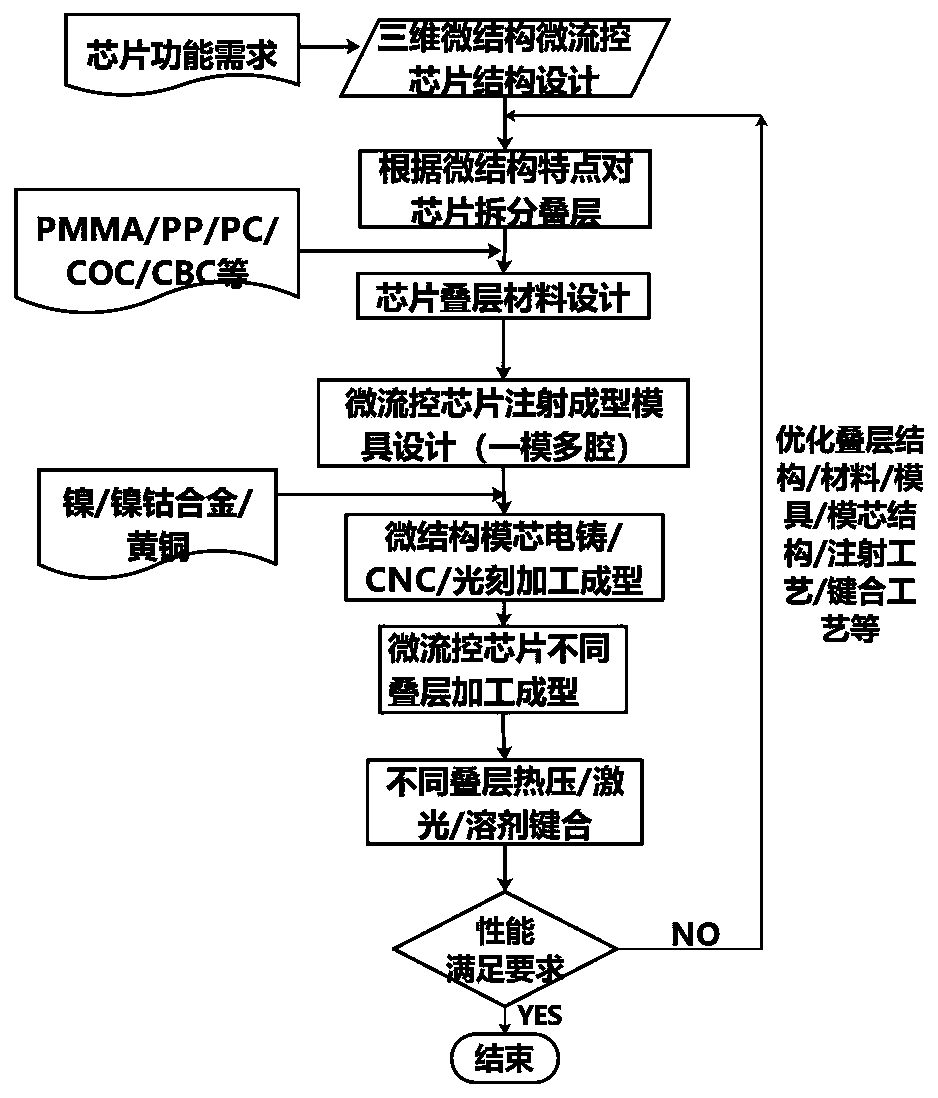
[0042] like figure 1 As shown, a method for manufacturing a three-dimensional microstructure polymer microfluidic chip, the specific steps are as follows:

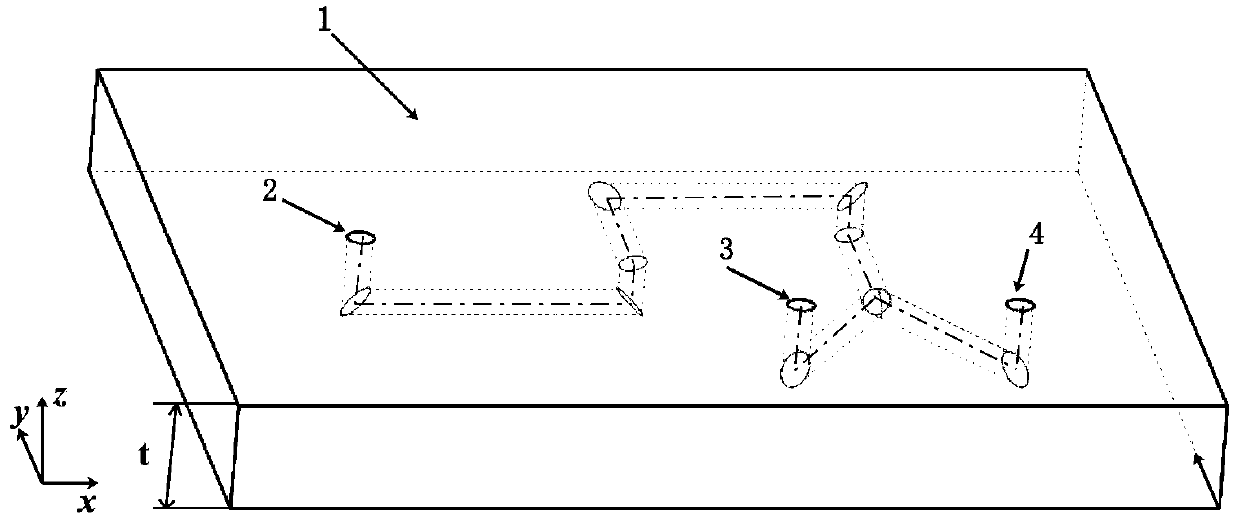
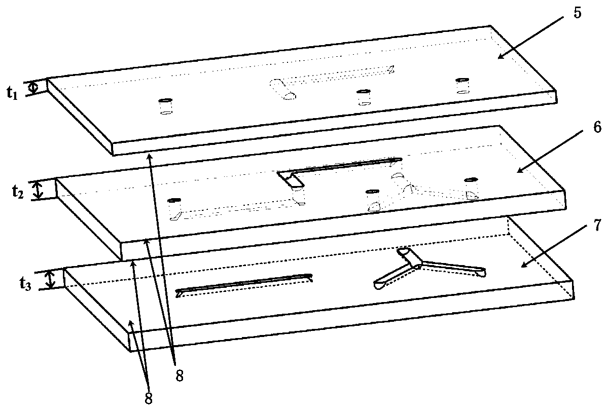
[0043] 1. Determine the microfluidic chip with three-dimensional microstructure according to the function of the chip, such as figure 2 shown. During the use of the chip, microfluid flow in three coordinates (x, y, z) directions can be realized. The chip has a solution inlet 2, a solution outlet I3, and a solution outlet II4. Structural analysis of the microfluidic chip with three-dimensional microstructure was carried out, and the chip was stacked and divided according to the number of x-direction channel planes in different z-directions of the chip. The chip is divided into three stacks, and the divided stacks are as follows image 3 As shown, including stack I5, stack II6 and stack III7. The split stack is as follows image 3 shown. There is a relationship t=t between the stack thickness and the total thickness ...

Embodiment 2

[0052] Make a three-dimensional microstructure microfluidic chip of PMMA material such as Figure 7 shown. Electroforming method is used to make different laminated mold cores, and the laminated layers are divided according to the structural characteristics such as Figure 7 As shown, it is divided into four laminates, and the ultrasonic micro-injection molding process is used for injection molding of different laminates. The injection-molded stacks are bonded by hot pressing or adhesive bonding to form a complete microfluidic chip with a three-dimensional microstructure, such as Figure 7 shown.


PUM


Abstract

The invention provides a laminated manufacturing method for three-dimensional microstructure polymer microfluidic chip. Three-dimensional microstructure microfluidic chips meeting design requirementsare split and laminated, different layers are separately processed, and a bonding process is used to achieve the molding of the three-dimensional microstructure polymer microfluidic chip. The method can realize the rapid, reliable and high-integration molding of the three-dimensional microstructure microfluidic chip, realizes the mass manufacturing of the three-dimensional microstructure microfluidic chip by optimizing all step processes, and effectively realizes the promotion and application of the three-dimensional microstructure microfluidic chip.

Description

technical field [0001] The invention relates to the technical field of microfluidic manipulation, in particular to a stacked manufacturing method of a polymer microfluidic chip with a three-dimensional microstructure. Background technique [0002] Microfluidic chips can realize the main functions of large-scale and multi-functional biochemical analysis laboratories. With their advantages of miniaturization, low consumption, rapid analysis and automation, they are widely used in disease diagnosis, food safety, epidemic control, environmental monitoring and other fields. In terms of structure, microfluidic chips need to form closed micro / nano channels to realize mixing, reaction, separation and other processes. The features of existing microfluidic chips such as micro-channels and micro-sections are mostly two-dimensional structures (the shape of the cross-section does not change at the height of the chip or shrinks linearly). With the continuous development of research relat...

Claims


Application Information

Patent Timeline
IPC IPC(8): B01L3/00B29C45/16B81C1/00
Inventor 蒋炳炎彭涛李湘林
Owner CENT SOUTH UNIV
Why Eureka
Eureka Blog
Learn More