A kind of encapsulation thin film and its preparation method, optoelectronic device
A technology for packaging films and organic films, applied in electrical components, semiconductor devices, circuits, etc., can solve the problems of poor water and oxygen barrier properties of packaging films, enhance water and oxygen barrier properties, meet the requirements of water vapor permeability, and improve the use of effect of life
- Summary
- Abstract
- Description
- Claims
- Application Information
AI Technical Summary
Problems solved by technology
Method used
Image

Examples
preparation example Construction
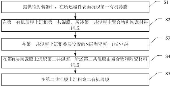
[0048] Further, the present invention also provides a method for preparing an encapsulation film, wherein, such as figure 2 shown, including steps:
[0049]S1. Providing a device to be packaged, and depositing a first organic thin film on the surface of the device;
[0050] S2. Depositing a first blended film on the first organic thin film, the first blended film is composed of a polymer and a ceramic material;
[0051] S3. Deposit N layers of ceramic films stacked on the first blend film, 1≤N≤4;
[0052] S4. Depositing a second blended film on the Nth layer of ceramic film, the second blended film is composed of a polymer and a ceramic material;
[0053] S5. Depositing a second organic thin film on the second blend film.
[0054] Further, the preparation of depositing the first mixed film on the first organic thin film includes the following steps:
[0055] Under alkaline conditions, the inorganic precursor and the organic monomer are reacted for the first time under an ...
Embodiment 1
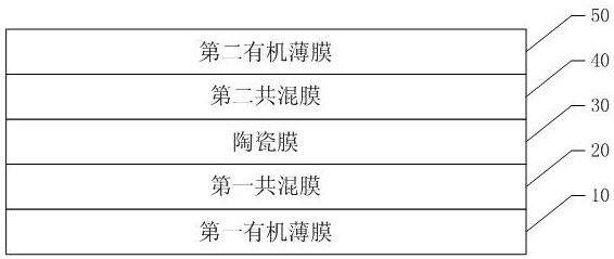
[0083] 1. The structure of the optoelectronic device is: ITO substrate / PEDOT:PSS (50 nm) / poly-TPD (30 nm) / quantum dot light-emitting layer (20 nm) / ZnO (30nm) / silver (70 nm) / encapsulation film (4100 nm), wherein the material of the packaging film is PLA / SiO 2 -PLA blend film / SiO 2 / SiO 2 -PLA blend film / PLA composite film, the SiO 2 The thickness of the film is 100nm, the thickness of the two layers of PLA film is 1000nm, and the thickness of the two layers of SiO 2 -The thickness of the PLA blend film is 1000nm.
[0084] 2. The packaging method of the optoelectronic device comprises steps:
[0085] 1) Cast a 10 mg / ml PLA chloroform solution on the top surface of the silver electrode of the optoelectronic device to form a film, and then vacuum dry it at 0.8 Pa at 120 °C for 30 min to prepare a PLA film;
[0086] 2) Under alkaline conditions, SiO with a mass fraction of 5 wt% 2 The alcohol solution and lactic acid were reacted in a nitrogen atmosphere at a ratio of 1:1, t...
Embodiment 2
[0091] 1. The structure of the optoelectronic device is: ITO substrate / PEDOT:PSS (50 nm) / poly-TPD (30 nm) / quantum dot light-emitting layer (20 nm) / ZnO (30nm) / silver (70 nm) / encapsulation film (9000 nm), wherein the material of the packaging film is PLA / SiO 2 -PLA blend film / SiO 2 / SiO 2 -PLA blend film / PLA composite film, the SiO 2The thickness of the film is 1000nm, the thickness of the two layers of PLA film is 3000nm, and the thickness of the two layers of SiO 2 -The thickness of the PLA blend film is 1000nm.
[0092] 2. The packaging method of the optoelectronic device comprises steps:
[0093] 1) Cast a 10 mg / ml PLA chloroform solution on the top surface of the silver electrode of the optoelectronic device to form a film, and then vacuum dry it at 0.8 Pa at 120 °C for 30 min to prepare a PLA film;
[0094] 2) Under alkaline conditions, SiO with a mass fraction of 20 wt% 2 The alcohol solution and lactic acid were reacted in a nitrogen atmosphere at a ratio of 1:1, ...
PUM
| Property | Measurement | Unit |
|---|---|---|
| thickness | aaaaa | aaaaa |
| thickness | aaaaa | aaaaa |
| thickness | aaaaa | aaaaa |
Abstract
Description
Claims
Application Information
 - R&D
- Intellectual Property
- Life Sciences
- Materials
- Tech Scout
- Unparalleled Data Quality
- Higher Quality Content
- 60% Fewer Hallucinations
Browse by: Latest US Patents, China's latest patents, Technical Efficacy Thesaurus, Application Domain, Technology Topic, Popular Technical Reports.
© 2025 PatSnap. All rights reserved.Legal|Privacy policy|Modern Slavery Act Transparency Statement|Sitemap|About US| Contact US: help@patsnap.com