Method for improving spacer shape

An isolation sidewall and isolation sidewall etching technology, applied in electrical components, semiconductor/solid-state device manufacturing, circuits, etc., can solve problems such as poly damage, achieve straight morphology, and increase the etching selectivity ratio.

Inactive Publication Date: 2019-07-05
SHANGHAI HUALI INTEGRATED CIRCUTE MFG CO LTD
View PDF4 Cites 0 Cited by
  • Summary
  • Abstract
  • Description
  • Claims
  • Application Information

AI Technical Summary

Problems solved by technology

[0004] The existing technology is to adjust the morphology of the isolation sidewall after the main etching. The only way to fine-tune the morphology of the sidewall is to remove the silicon nitride on the wafer surface through over-etching. Due to the film quality of the poly top and the sidewall With the same limitation, when the sidewall CD is adjusted by over-etching, the top of the Poly will also produce obvious shoulder loss, and over-etching may even cause damage to the Poly.

Method used


Image

  • Method for improving spacer shape
  • Method for improving spacer shape
  • Method for improving spacer shape

Examples


no. 1 example

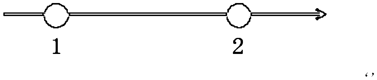
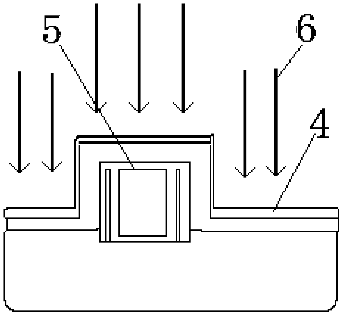
[0028] Such as figure 2 As shown, the present invention provides a first embodiment of a method for improving the morphology of isolation spacers in the production of semiconductor devices, including:

[0029] 1) Deposit the isolation side wall film;

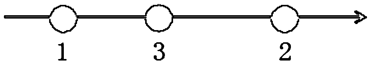
[0030] 2) Perform plasma anisotropic bombardment, the angle of the plasma anisotropic bombardment is vertical bombardment from the top of the device to the bottom, refer to image 3 shown;

[0031] 3) Depositing the isolation side wall film again;

[0032] 4) Then perform isolation spacer etching.

[0033] Wherein, the spacer film is a nitride film, and the plasma is nitrogen, chlorine, hydrogen chloride, bromine or hydrogen bromide.

no. 2 example

[0034] The present invention provides a second embodiment of a method for improving the morphology of isolation sidewalls in the production of semiconductor devices, including:

[0035] 1) Deposit the isolation side wall film;

[0036] 2) Perform plasma anisotropic bombardment, the angle of the plasma anisotropic bombardment is vertical bombardment from the top of the device to the bottom, refer to image 3 shown;

[0037] Wherein, the plasma anisotropic bombardment pressure is 5mt-10mt, preferably 6mt, 7mt, 8mt or 9mt.

[0038] The power of the plasma anisotropic bombardment source is 400W-700W, preferably 500W or 600W.

[0039] The plasma anisotropic bombardment bias voltage is 100V-200V, preferably 150V.

[0040] 3) Depositing the isolation side wall film again;

[0041] 4) Then perform isolation spacer etching.

[0042] Wherein, the spacer film is a nitride film.

no. 3 example

[0043] The present invention provides a third embodiment of a method for improving the morphology of isolation sidewalls in the production of semiconductor devices, including:

[0044] 1) Depositing an isolation spacer film; the isolation spacer film is a nitride film.

[0045] 2) Perform plasma anisotropic bombardment, the angle of the plasma anisotropic bombardment is vertical bombardment from the top of the device to the bottom, refer to image 3 shown;

[0046] Wherein, the plasma is nitrogen, chlorine, hydrogen chloride, bromine or hydrogen bromide.

[0047] The plasma anisotropic bombardment pressure is 5mt-10mt, preferably 6mt, 7mt, 8mt or 9mt.

[0048] The power of the plasma anisotropic bombardment source is 400W-700W, preferably 500W or 600W.

[0049] The plasma anisotropic bombardment bias voltage is 100V-200V, preferably 150V.

[0050] 3) Depositing the isolation side wall film again;

[0051] 4) Then perform isolation sidewall etching;

[0052] The etching g...


PUM


Abstract

The invention discloses a method for improving a spacer shape in the production of a semiconductor device. The method comprises steps of: depositing a spacer film, performing plasma anisotropic bombardment, re-depositing the spacer film, and then performing the spacer etching. The method utilizes plasma anisotropic bombardment before etching the spacer of the semiconductor device, and bombards thedevice in the vertical direction by plasma. The contact area between the spacer and the plasma is different from that between the top of the polycrystalline silicon and the plasma in the vertical direction, thereby increasing an etching selection ratio between the spacer and a nitride film on the top of the polycrystalline silicon, and achieving less shoulder loss and a more straight shape of thespacer.

Description

technical field [0001] The invention relates to the field of semiconductor manufacturing, in particular to a method for improving the shape of the isolation side wall. Background technique [0002] In the manufacturing technology of semiconductor integrated circuits, etching of spacers is one of the key steps. With the development of integrated circuit technology, the sensitivity and requirements of semiconductor device performance to spacer uniformity are further increased. [0003] However, the etching of the isolation sidewall has poor control over the edge of the sidewall, making it very difficult to control the thickness of the edge sidewall, and the etching rate of the isolation sidewall is inconsistent. This difference is due to the poor uniformity of the sidewall surface and the isolation The sidewall morphology is poor, which in turn leads to poor overall device uniformity. figure 1 It is a manufacturing method for isolating sidewalls of semiconductor devices in t...

Claims


Application Information

Patent Timeline
IPC IPC(8): H01L21/311
CPCH01L21/31116H01L21/31144
Inventor 姜林鹏陆连李全波
Owner SHANGHAI HUALI INTEGRATED CIRCUTE MFG CO LTD
Why Eureka
Try Eureka