A silicon wafer automatic slice feeding mechanism

A technology of silicon wafers and feeding mechanism, which is applied to conveyor objects, electrical components, transportation and packaging, etc., can solve problems such as broken silicon wafers, and achieve the effect of uniform size, good verticality and ingenious structure

Active Publication Date: 2020-04-07
浙江金麦特自动化系统有限公司
View PDF4 Cites 0 Cited by
  • Summary
  • Abstract
  • Description
  • Claims
  • Application Information

AI Technical Summary

Problems solved by technology

[0005] However, the above-mentioned patent directly makes the silicon wafer output in pieces through the friction between the rubber hose and the silicon wafer, and the rotation of the rubber hose can easily cause the silicon wafer to break

Method used


Image

  • A silicon wafer automatic slice feeding mechanism
  • A silicon wafer automatic slice feeding mechanism
  • A silicon wafer automatic slice feeding mechanism

Examples


Embodiment 1

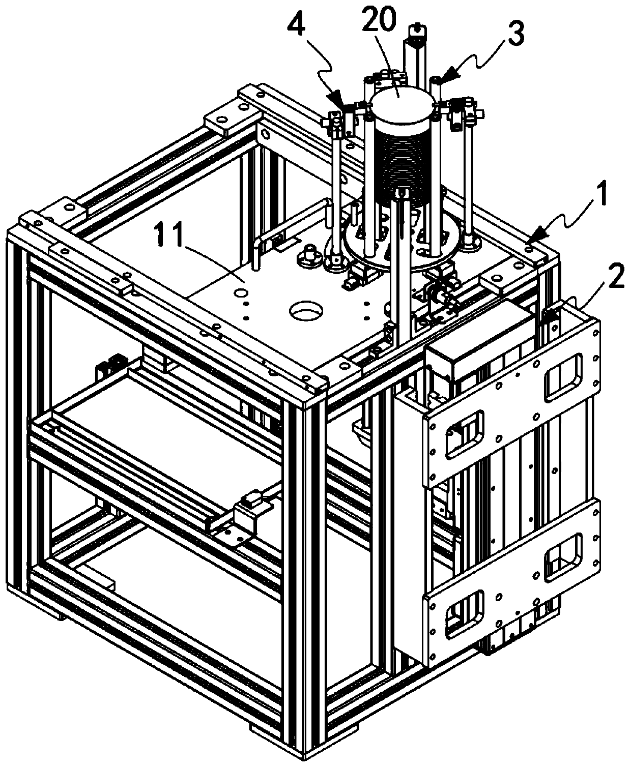
[0059] like Figure 1 to Figure 6 Shown, a kind of silicon wafer automatic slicing feeding mechanism comprises:

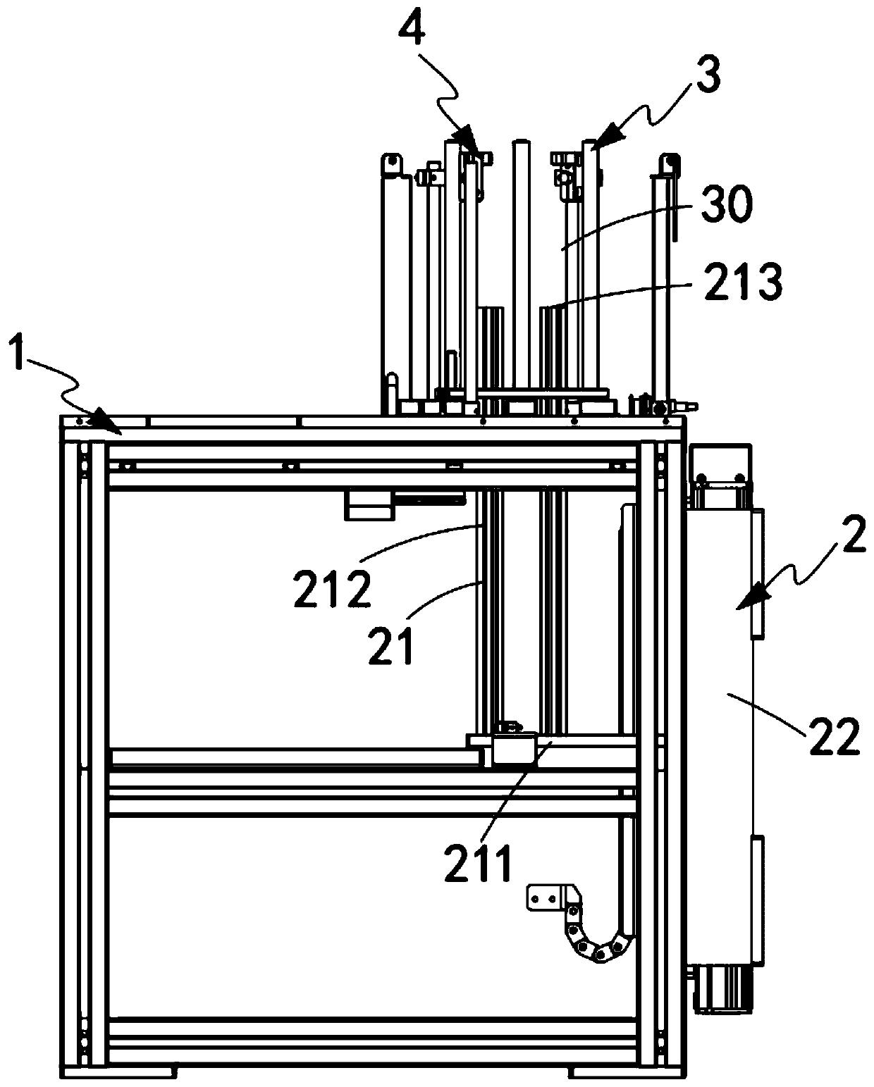
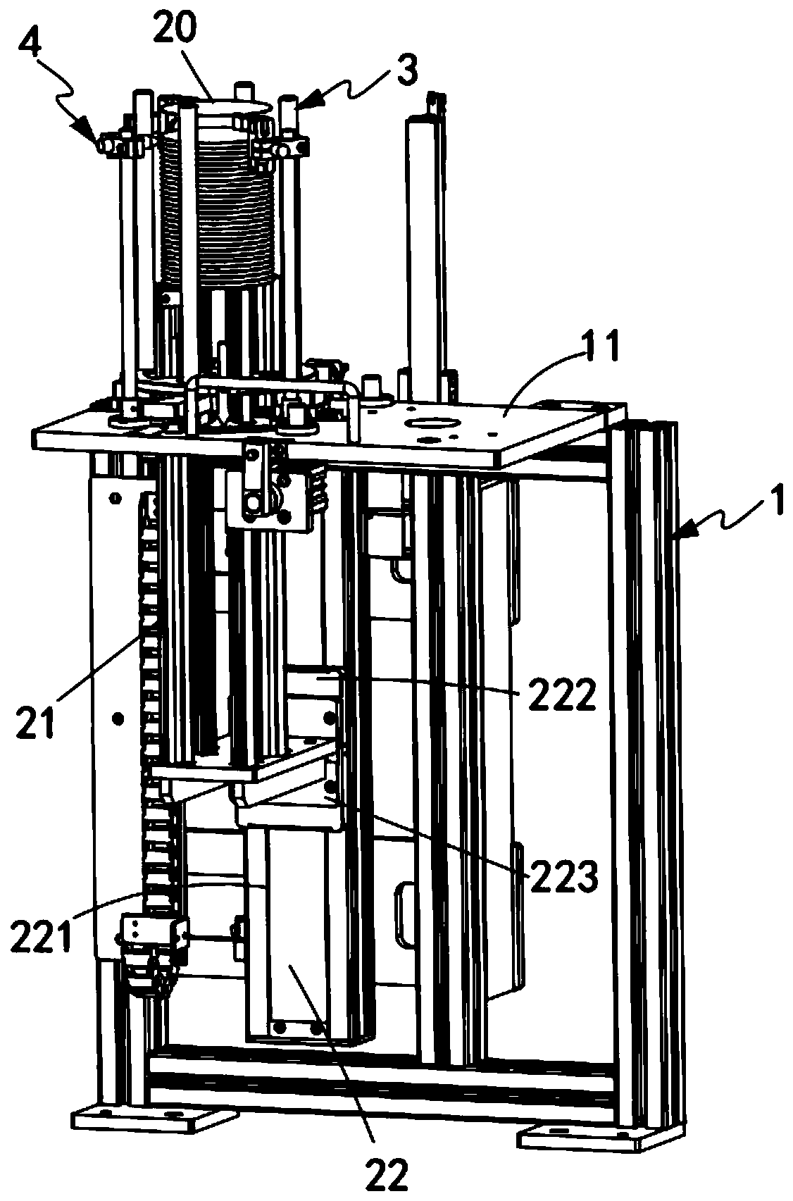
[0060] Installation frame 1, the top of described installation frame 1 is provided with workbench 11;

[0061] The feeding mechanism 2 vertically penetrates the workbench 11 and is installed on the installation frame 1, which includes a support assembly 21 and a lifting assembly 22, and the top of the support assembly 21 is stacked with silicon wafers 20. The lifting assembly 22 drives the silicon wafer 20 to lift;

[0062] The limit mechanism 3, the limit mechanism 3 is arranged on the workbench 11, it is arranged around the support assembly 21, and it includes a plurality of limit rods 31 arranged in parallel sliding, between the limit rods 31 forming a material area 30 for stacking the silicon wafers 20; and

[0063] Layering mechanism 4, described layering mechanism 4 is installed on the top of described material area 30, and it divides and is positioned at ...

Embodiment approach

[0067] like figure 2 As shown, as a preferred embodiment, the support assembly 21 includes:

[0068] The mounting plate 211, the mounting plate 211 is horizontally arranged, it is connected with the lifting assembly 22, and it is driven by the lifting assembly 22 to lift and set in the vertical direction; and

[0069] Support rods 212, several of the support rods 212 are installed vertically on the mounting plate 211, the support rods 212 are equidistantly arranged along the lifting direction of the mounting plate 211, and the tops of the support rods 212 are matched to form A placement platform 213 for placing the silicon wafer 20 .

[0070] It should be noted that the number of support rods 212 in the present invention is preferably four, and the tops of the support rods 212 are arranged flat to form a placing platform 213 on which silicon wafers 20 are stacked.

[0071] like image 3 and Figure 4 As shown, as a preferred embodiment, the lifting assembly 22 includes: ...

Embodiment 2

[0096] Figure 10 It is a schematic structural view of Embodiment 2 of a silicon wafer automatic slice feeding mechanism of the present invention; as Figure 10As shown, the parts that are the same as or corresponding to those in Embodiment 1 use the reference numerals corresponding to Embodiment 1. For the sake of simplicity, only the differences from Embodiment 1 will be described below. This embodiment two and figure 1 The difference of the shown embodiment one is:

[0097] like Figure 10 and Figure 11 As shown, a silicon wafer automatic slice feeding mechanism, one side of the limit mechanism 3 is provided with a buffer mechanism 5, and the buffer mechanism 5 is arranged on the workbench 11, which includes:

[0098] A blanking container 51, a buffer liquid is contained in the blanking container 51;

[0099] A discharge handle 52, the discharge handle 52 is placed in the discharge container 51, and it is detachably arranged; and

[0100] An overflow container 53, th...


PUM


Abstract

The invention provides an automatic silicon wafer separating and feeding mechanism. The automatic silicon wafer separating and feeding mechanism comprises an installation machine frame, a feeding mechanism, a limiting mechanism and a layering mechanism; a workbench is arranged on the top of the installation machine frame; the feeding mechanism vertically passes through the workbench; the feeding mechanism comprises a support assembly and a lifting assembly; the limiting mechanism is arranged by surrounding the support assembly; the layering mechanism is installed on the top of a material areaformed by the limiting mechanism; a hairbrush is matched with the lifting assembly, so that a silicon wafer stacking material arranged in a vertical lifting manner is driven; by utilization of the hairbrush, the silicon wafer on the top of the silicon wafer stacking material is separated from the stacking material; simultaneously, by utilization of an air nozzle, a silicon wafer at the topmost position is separated from a tightly adjacent silicon wafer below, so that a buffer area is formed; therefore, when a vacuum chuck downwardly moves to adsorb the silicon wafer, a downward buffer intervalexists; the silicon wafers are prevented from being extruded and crushed; the technical problem that the silicon wafers are pressurized and easily crushed when being grabbed can be solved; and automatic and one-by-one orderly separating and output of the silicon wafers can be realized.

Description

technical field [0001] The invention relates to the technical field of silicon wafer automatic feeding machinery, in particular to a silicon wafer automatic slice feeding mechanism. Background technique [0002] As a good conductive material, silicon wafer can be widely used in technical fields such as semiconductors and solar cells. In the later stage of the silicon wafer processing process, steps such as chamfering, grinding, corrosion, polishing and cleaning are generally required. Cleaning refers to liquid cleaning of the processed silicon wafer to remove impurities on the surface of the silicon wafer, so as to avoid scratches on the surface of the silicon wafer, cracking, etc., is therefore a very important process step. [0003] However, the silicon wafer cleaning machine in the prior art is more complicated to operate, and the silicon wafer needs to be manually placed in the cleaning tank for cleaning, and the silicon wafer is fragile, and it is very easy to break du...

Claims


Application Information

Patent Timeline
Patent Type & Authority Patents(China)
IPC IPC(8): H01L21/677
CPCH01L21/67739H01L21/67778
Inventor 江帆周杰史强大
Owner 浙江金麦特自动化系统有限公司
Why Eureka
Try Eureka