

Semiconductor structure and formation method thereof
A technology of semiconductor and gate structure, applied in the field of semiconductor structure and its formation, can solve problems such as poor performance of vertical nanowire transistors, and achieve the effects of reduced etching, high integration and simple etching process
- Summary
- Abstract
- Description
- Claims
- Application Information
AI Technical Summary
Problems solved by technology
Method used
Image

Examples
Embodiment Construction
[0038] There are many problems in the semiconductor structure in the prior art, for example, the performance of the semiconductor structure is poor.
[0039] Now in combination with a semiconductor structure, the reasons for the poor performance of the semiconductor structure are analyzed:
[0040] Due to the large substrate surface occupied by conventional planar transistors, the integration degree of the semiconductor structure is low. In order to increase the integration degree of the formed semiconductor structure, a vertical nanowire transistor is proposed.
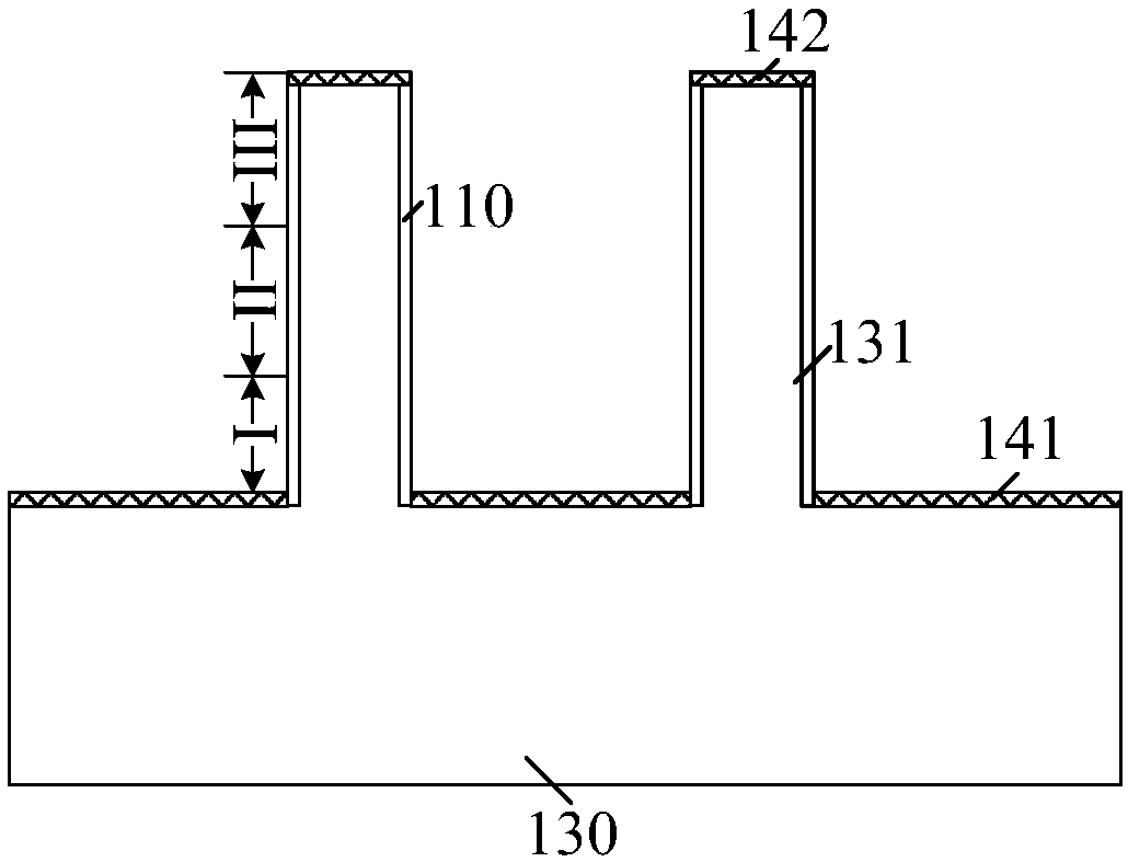
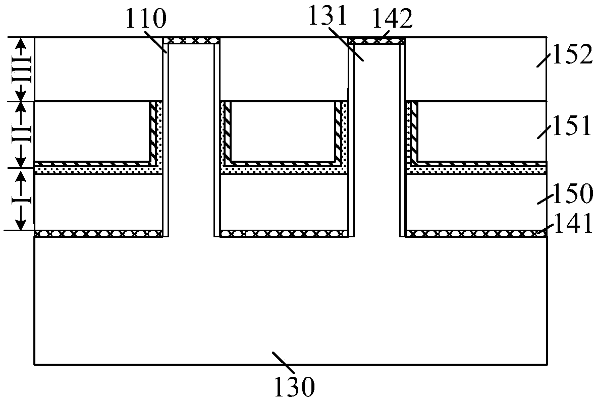
[0041] figure 1 and figure 2 It is a structural schematic diagram of each step of a method for forming a vertical nanowire transistor.
[0042] Please refer to figure 1 , a substrate 130 is provided, the surface of the substrate 130 has a fin post 131, and the fin post 131 includes a bottom region I, a channel region II on the bottom region I, and a top portion on the channel region II Zone III.
[0043] conti...
PUM
| Property | Measurement | Unit |
|---|---|---|
| Thickness | aaaaa | aaaaa |
| Thickness | aaaaa | aaaaa |
Abstract
Description
Claims
Application Information