
Integrated gate commutation thyristor device with high current impact tolerance capability

A technology for commutating thyristors and gate commutation, which is applied to electrical components, semiconductor devices, circuits, etc. Thyristor effective resistivity reduction and other issues

Pending Publication Date: 2019-07-05
TSINGHUA UNIV
View PDF0 Cites 2 Cited by
  • Summary
  • Abstract
  • Description
  • Claims
  • Application Information

AI Technical Summary

Problems solved by technology

Although the introduction of anode reactance can not only avoid the failure of the opening process, but also effectively limit the short-circuit current and short-circuit energy after the device fails, but the current impact (current impact is the differential operation dI / dt of the current intensity I in the device to the time t , where, I represents the current intensity in the device, t represents the time) tolerance leads to the excessive volume of the IGCT series anode reactance, which brings great difficulties to the equipment volume, mechanical structure and heat dissipation design in the application.
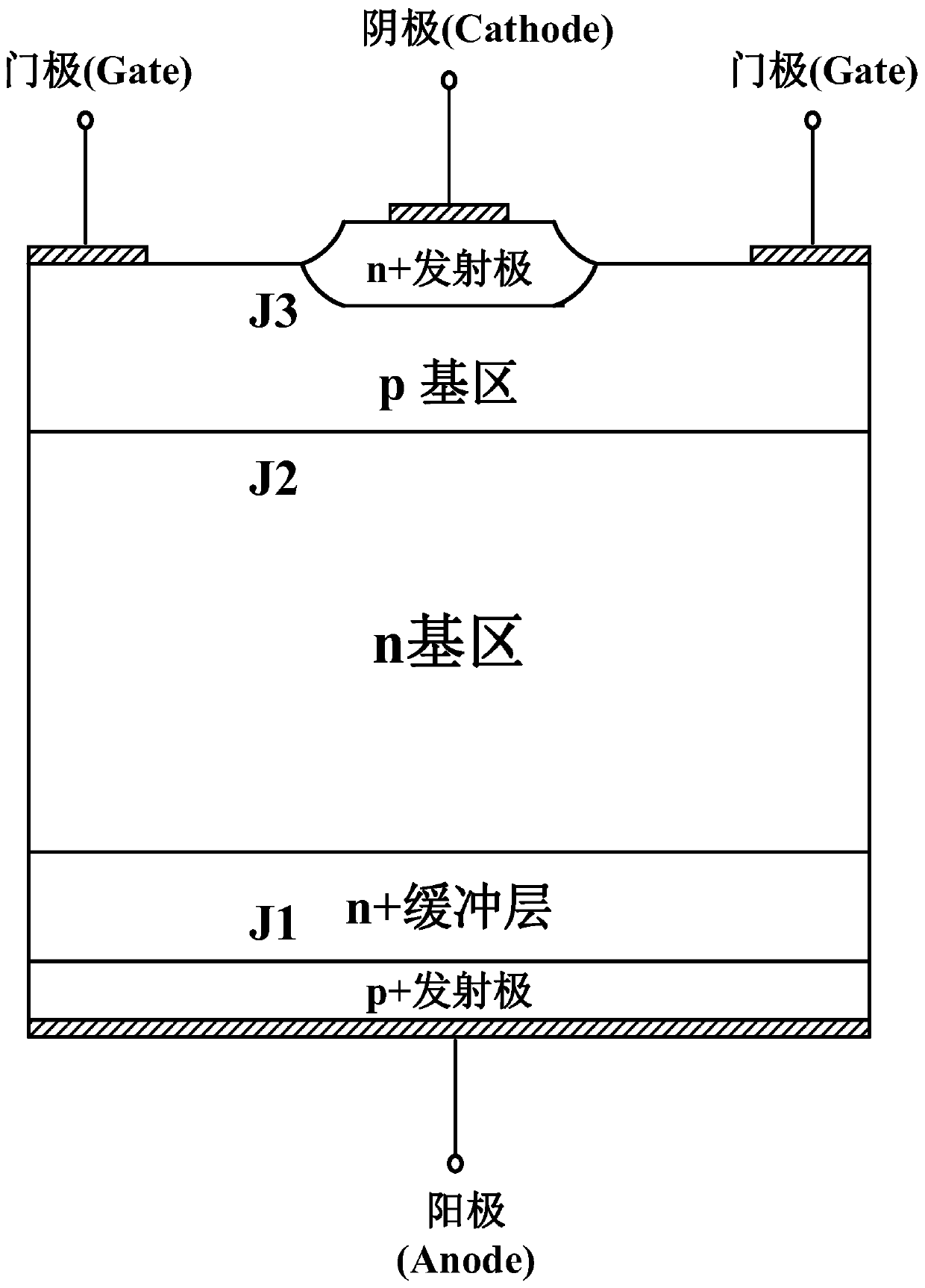
[0004] figure 1 Shown is a typical structure of a gate-commutated thyristor (GCT) chip unit. During the triggered conduction of the gate-commutated thyristor, the gate drive injects current from the gate to the cathode, and electrons are emitted from the cathode emitter , and diffuse to the anode side and the lower area of ​​the gate, the local electric field caused by crossing the J2 depletion region will cause hole emission on the anode side, triggering the device to enter the conductance modulation state, so that the effective resistivity inside the gate commutation thyristor decrease, resulting in an increase in the current intensity in the gate-commutated thyristor, and the gate-commutated thyristor is subject to current impact, and the above-mentioned device failure is prone to occur

Method used


Image

  • Integrated gate commutation thyristor device with high current impact tolerance capability
  • Integrated gate commutation thyristor device with high current impact tolerance capability
  • Integrated gate commutation thyristor device with high current impact tolerance capability

Examples


Embodiment Construction

[0030] In order to make the objects, technical solutions and advantages of the present invention more apparent, exemplary embodiments according to the present invention will be described in detail below with reference to the accompanying drawings. Apparently, the described embodiments are only some embodiments of the present invention, rather than all embodiments of the present invention, and it should be understood that the present invention is not limited by the exemplary embodiments described here. Based on the embodiments described herein, all other embodiments obtained by those skilled in the art without creative effort shall fall within the protection scope of the present invention. In this specification and the drawings, substantially the same elements and functions will be denoted by the same reference numerals, and repeated descriptions of these elements and functions will be omitted. Also, descriptions of functions and constructions that are well known in the art may...


PUM

PropertyMeasurementUnit
Horizontal sizeaaaaaaaaaa

Abstract

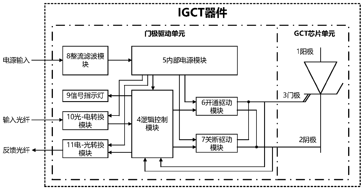
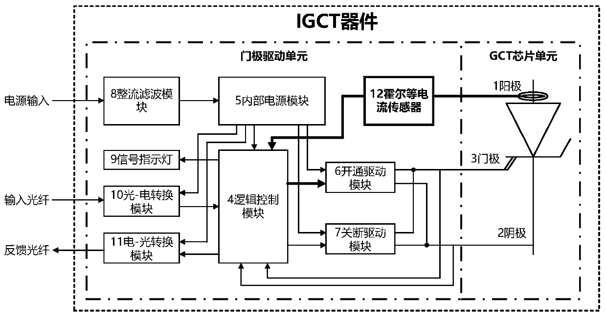
The invention provides an integrated gate commutation thyristor device with high current impact (dI / dt) tolerance capability. The device comprises a gate commutation thyristor chip unit and a gate drive unit, wherein the integrated gate commutation thyristor device also comprises one or more of the following components of: a gate drive unit having a triggering current increasing to 10A, a gate commutation thyristor chip having an internal carrier service life being larger than 100us, a gate contact ring cathode surface structure with the cathode current density approximately equal in each areaof the chip, and a single gate commutation thyristor unit with the transverse size shortened to be within 200 um. The integrated gate commutation thyristor device can be fully conducted without beingdamaged under the condition of the high current impact, the anode reactance for limiting the current rising speed in system application is effectively reduced, the volume of an external module is reduced, and the convenience in the application is improved.

Description

technical field [0001] The invention belongs to the technical field of semiconductor integrated circuits, and in particular relates to an integrated gate commutated thyristor (IGCT) device with high current impact withstand capability. Background technique [0002] For bipolar devices represented by thyristors, gate turn-off thyristors (GTOs), and IGCTs, during the turn-on process, since carriers need to diffuse laterally to generate conductive plasma in the semiconductor body, the given gate A certain time delay is required after the trigger signal to achieve sufficient turn-on. However, in the circuit, after the voltage between the cathode and anode of the power electronic device drops, the current level is mainly affected by the topology and parameters of the outer loop. When the resistance and inductance in the loop are small, the current often rises at a speed of up to kA / us. In this process, if the carriers in the device are not fully diffused and turned on, it is eas...

Claims


Application Information

Patent Timeline
IPC IPC(8): H01L29/744H01L29/423
CPCH01L29/744H01L29/42356
Inventor 刘佳鹏曾嵘周文鹏赵彪余占清陈政宇
Owner TSINGHUA UNIV
Learn More