A substrate transfer mechanism, photolithography machine and substrate transfer method

A substrate and adapter plate technology, applied in microlithography exposure equipment, optics, optomechanical equipment, etc., can solve the problems of poor control of the lift of the ejector pin, redundant thickness of the substrate carrier, and high measurement and detection requirements. To achieve the effect of shortening handover time, compact structure, handover efficiency and safety

Active Publication Date: 2021-03-19
SHANGHAI MICRO ELECTRONICS EQUIP (GRP) CO LTD
View PDF4 Cites 0 Cited by
  • Summary
  • Abstract
  • Description
  • Claims
  • Application Information

AI Technical Summary

Problems solved by technology

[0003] Subsequently, the measurement and inspection requirements for the substrate used to manufacture integrated circuits are getting higher and higher, especially when measuring the critical dimensions of the substrate or detecting manufacturing defects, etc., the substrate often needs to be rotated at a large angle, which gives Substrate handover mechanisms present difficulties
[0004] In the existing substrate measurement and detection technology, the substrate handover device or the groove is directly made on the substrate carrier, but the vertical lifting stroke during the handover process of the substrate transport manipulator is limited, and if the groove on the substrate carrier is added The depth of the base carrier will produce redundant thickness in the vertical direction; or add the ejector pin detachment means, after the transfer of the base, the ejector pin will be separated from the base carrier, but the stroke of the ejector pin includes the base carrier The thickness dimension is a redundant stroke, and there is a risk of collision with the base carrier when the ejector pin is extended; or the ejector pin is driven up and down by a clutch, and when the ejector pin is lowered, it is separated from the lifting drive unit , can be rotated together by the base carrier, but the lifting and lowering of the ejector pin is not easy to control, especially the uncontrollable descending speed, which makes the base transfer accuracy of this structure not enough, and even has potential safety hazards

Method used


Image

  • A substrate transfer mechanism, photolithography machine and substrate transfer method
  • A substrate transfer mechanism, photolithography machine and substrate transfer method
  • A substrate transfer mechanism, photolithography machine and substrate transfer method

Examples


Embodiment Construction

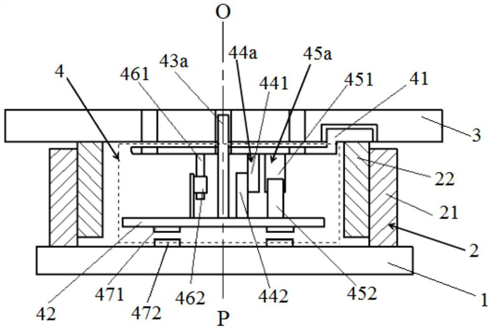
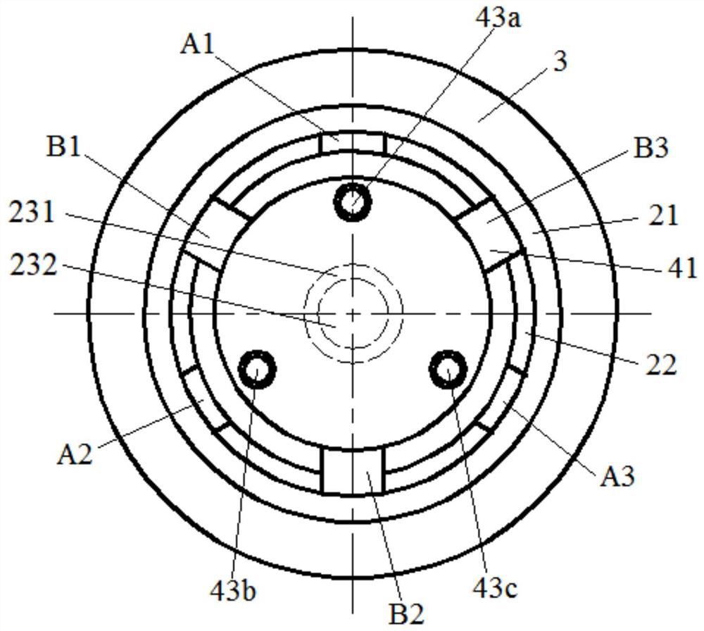
[0040] The specific implementation manner of the present invention will be described in more detail below with reference to schematic diagrams. Advantages and features of the present invention will be apparent from the following description and claims. It should be noted that all the drawings are in a very simplified form and use imprecise scales, and are only used to facilitate and clearly assist the purpose of illustrating the embodiments of the present invention.

[0041] After studying the following three types of substrate transfer devices that can rotate at a large angle, the inventors found that:

[0042] (1) Grooves are directly made on the base carrier, but the vertical lifting stroke during the handover process of the substrate transfer manipulator is limited, and if the depth of the groove on the base carrier is increased, the substrate carrier will be redundant in the vertical direction. excess thickness;

[0043](2) Add the ejector pin detachment means. After th...


PUM


Abstract

Disclosed are a substrate transfer mechanism, a photoetching machine and a substrate transfer method, wherein the substrate transfer mechanism comprises a base (1), a rotation driving unit (2), a lifting driving unit (4) and a substrate carrier (3). The rotation driving unit (2) is arranged on the base (1), the substrate carrier (3) is arranged on the rotation driving unit (2), the lifting driving unit (4) is located below the substrate carrier (3), and the lifting driving unit (4) rotates along with the substrate carrier (3). The lifting driving unit (4) comprises a lifting driving motor (45a), ejection pins (43a, 43b, 43c) and a lifting guiding module (44a), the lifting driving motor (45a) driving the ejection pins (43a, 43b, 43c) to pass through the substrate carrier (3) to perform lifting, and the lifting guiding module (44a) directing a lifting direction of the ejection pins (43a, 43b, 43c). The substrate transfer mechanism can realize a large-angle rotation of a substrate, and has high transfer precision and efficiency, high reliability, a compact structure, a small spatial occupied size, and almost has no transfer lifting redundant stroke and transfer impact risk, and has high transfer security.

Description

technical field [0001] The invention relates to the technical field of integrated circuit manufacturing, in particular to a substrate transfer mechanism, a photolithography machine and a substrate transfer method. Background technique [0002] After experiencing the development stages of small-scale integration (SSI), medium-scale integration (MSI) and large-scale integration (LSI), integrated circuit manufacturing technology has now entered the stage of very large-scale integration (VLSI) and ultra-large-scale integration (ULSI). , The scale of integration has grown from a few transistors on a single substrate to tens of millions or even hundreds of millions of transistors on one substrate. The characteristic line width that marks the level of integrated circuit technology has also developed from tens of microns for small-scale integrated circuits to today's ultra-deep submicron (VDSM) level, and the diameter of the substrate has gradually changed from 2 inches, 3 inches, 4...

Claims


Application Information

Patent Timeline
Patent Type & Authority Patents(China)
IPC IPC(8): G03F7/20
CPCG03F7/70716G03F7/70733G03F7/20H01L21/683
Inventor 吴文娟
Owner SHANGHAI MICRO ELECTRONICS EQUIP (GRP) CO LTD
Why Eureka
Try Eureka