Thin film encapsulation structure, OLED (organic light emitting diode) display panel and manufacturing method thereof
A thin-film encapsulation and display panel technology, applied in semiconductor/solid-state device manufacturing, electrical components, electrical solid-state devices, etc., can solve problems such as loss and aging, decrease in the ability of organic film layers to buffer stress, and limit the service life of foldable mobile phones, etc. Achieve the effect of avoiding wear and aging and improving bending ability
- Summary
- Abstract
- Description
- Claims
- Application Information
AI Technical Summary
Problems solved by technology
Method used
Image

Examples
Embodiment Construction
[0036] The following descriptions of the various embodiments refer to the accompanying drawings to illustrate specific embodiments in which the invention may be practiced. The directional terms mentioned in the present invention, such as [top], [bottom], [front], [back], [left], [right], [inside], [outside], [side], etc., are only for reference The orientation of the attached schema. Therefore, the directional terms used are used to illustrate and understand the present invention, but not to limit the present invention. In the figures, structurally similar elements are denoted by the same reference numerals.
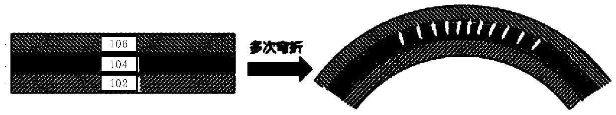
[0037] First, the prior art is briefly described. see figure 1 , figure 1 It is a comparative schematic diagram of the thin film packaging structure in the prior art before and after bending. Existing thin film packaging structures often include a film layer structure composed of a first inorganic thin film 102 , a first organic thin film 104 and a second inorganic ...
PUM
 Abstract
Description
Claims
Application Information
 - Generate Ideas
- Intellectual Property
- Life Sciences
- Materials
- Tech Scout
- Unparalleled Data Quality
- Higher Quality Content
- 60% Fewer Hallucinations
Browse by: Latest US Patents, China's latest patents, Technical Efficacy Thesaurus, Application Domain, Technology Topic, Popular Technical Reports.
© 2025 PatSnap. All rights reserved.Legal|Privacy policy|Modern Slavery Act Transparency Statement|Sitemap|About US| Contact US: help@patsnap.com