Flip-chip light emitting diode chip and method of manufacturing flip-chip light emitting diode chip

A technology for light-emitting diodes and chips, applied in electrical components, circuits, semiconductor devices, etc., can solve the problems of complicated and cumbersome processes, short-circuiting of P electrodes, and high production costs, shortening the lithography process, reducing the manufacturing process, and improving the work reliability. Effect

Pending Publication Date: 2019-08-02
ELEC TECH PHOTOELECTRIC TECH DALIAN
View PDF0 Cites 4 Cited by
  • Summary
  • Abstract
  • Description
  • Claims
  • Application Information

AI Technical Summary

Problems solved by technology

[0004] Based on this, it is necessary to provide a simple and time-consuming production method for the problems that the traditional flip-chip LED chip is prone to cracks and causes short-circuiting of the P electrode and the N electrode. Flip-chip light-emitting diode chip preparation method and light-emitting diode chip that are short, low in production cost, and have no risk of leakage

Method used


Image

  • Flip-chip light emitting diode chip and method of manufacturing flip-chip light emitting diode chip
  • Flip-chip light emitting diode chip and method of manufacturing flip-chip light emitting diode chip
  • Flip-chip light emitting diode chip and method of manufacturing flip-chip light emitting diode chip

Examples


Embodiment Construction

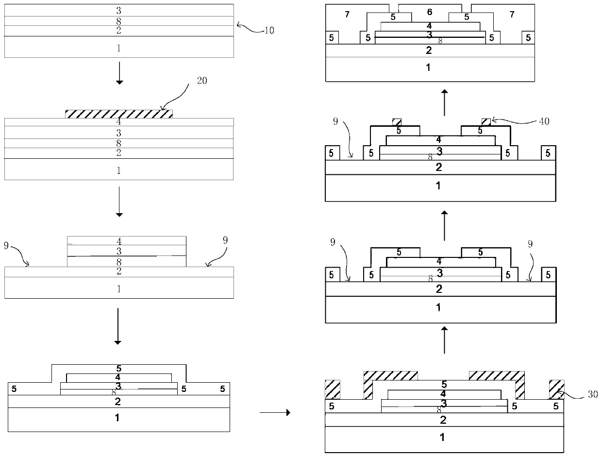
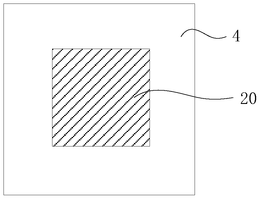
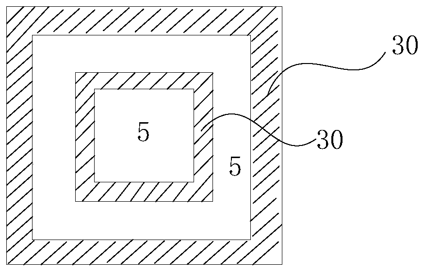
[0028] In order to make the purpose, technical solution and advantages of the present application clearer, the present application will be further described in detail through the following embodiments and in conjunction with the accompanying drawings. It should be understood that the specific embodiments described here are only used to explain the present application, not to limit the present application.

[0029] The serial numbers assigned to components in this document, such as "first", "second", etc., are only used to distinguish the described objects, and do not have any sequence or technical meaning. The "connection" and "connection" mentioned in this application all include direct and indirect connection (connection) unless otherwise specified. In the description of this application, it should be understood that the terms "upper", "lower", "front", "rear", "left", "right", "vertical", "horizontal", "top", The orientation or positional relationship indicated by "bottom"...


PUM


Abstract

The invention provides a flip-chip light emitting diode chip and a method of manufacturing the flip-chip light emitting diode chip. An N-type metal electrode layer extends to the edge of an N-type semiconductor step. A light emitting layer, a P-type semiconductor layer and a transparent conductive layer are disposed in a middle portion of the flip-chip light emitting diode chip, and thus, a Mesa step (a quantum well) is away from the edge of the chip. When crack breakage happens to the edge of the flip-chip light emitting diode chip and solder paste is connected with a P or N pole, short circuit of a P-type metal electrode layer and an N-type metal electrode layer is not caused, and leakage failure does not occur. Through three times of photoetching of the flip-chip light emitting diode chip manufacturing method, the number of photoetching processes is reduced, the use cost of raw materials such as a photoresist and a developer involved in the photoetching process can be saved, and theyield loss brought by photoresist residue can be effectively improved.

Description

technical field [0001] The present application relates to the technical field of semiconductors, in particular to a flip-chip light-emitting diode chip and a method for preparing a flip-chip light-emitting diode chip. Background technique [0002] A light emitting diode (Light Emitting Diode, LED) converts electrical energy into light energy, and emits visible light of various colors such as yellow, green, and blue, as well as infrared and ultraviolet invisible light. Compared with incandescent lamps and neon lamps, LEDs have the advantages of low operating voltage and current, high reliability, long life and convenient adjustment of luminous brightness. [0003] With the outbreak of the LED lamp market approaching, the research and development competition of LED packaging technology is also very fierce. At present, GaN-based LED chips are mainly divided into two types: front-mount structure and flip-chip structure. The light emitted by the positive structure is emitted th...

Claims


Application Information

Patent Timeline
Patent Type & Authority Applications(China)
IPC IPC(8): H01L33/38H01L33/10H01L33/20H01L33/00
CPCH01L33/007H01L33/10H01L33/20H01L33/385H01L2933/0016
Inventor 刘岩闫宝玉刘鑫鲁洋刘宇轩陈顺利
Owner ELEC TECH PHOTOELECTRIC TECH DALIAN
Why Eureka
Try Eureka