

Silicon dioxide SAB removing method
A silicon dioxide and wafer technology, applied in electrical components, semiconductor/solid-state device manufacturing, circuits, etc., can solve problems such as over-etching, leakage, and difficult to remove
- Summary
- Abstract
- Description
- Claims
- Application Information
AI Technical Summary
Problems solved by technology
Method used
Image

Examples
no. 1 example
[0024] The silicon dioxide SAB removal method of this embodiment includes the following steps.
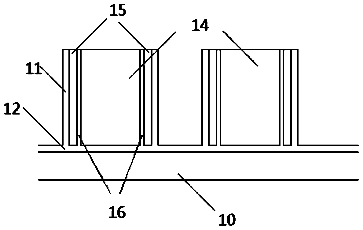
[0025] Step S01 , providing a flash memory chip on which devices are covered by silicon dioxide SAB.
[0026] Wherein, the devices in this step include, but are not limited to, memory cell Cell regions and high-voltage devices, and these devices are all covered by silicon dioxide SAB.
[0027] Step S02, use NH 3 Reacts with HF vapor and the silicon dioxide SAB on the flash chip to generate (NH 4 ) 2 SiF 6 .
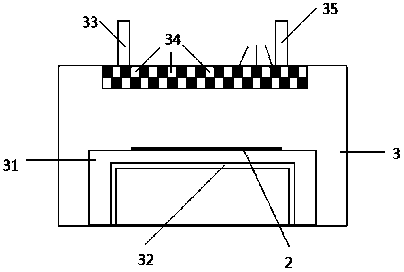
[0028] Wherein, the reaction temperature of this step is room temperature, i.e. 25°C, which is realized by the following settings: figure 2 As shown, the above-mentioned flash memory chip 2 is placed on the first reaction platform 31 in the first reaction chamber 3. The first reaction platform 31 has a built-in constant temperature water pipe 32, which is passed to the first reaction platform by circulating water at 25°C. 31 surface, so that the flash memory chip 2 is k...
PUM
 Abstract
Description
Claims
Application Information