Method for preparing GaN-based inversely-installed thin film structure near-ultraviolet LED

A thin film structure, near-ultraviolet technology, applied in the field of optoelectronics, can solve the problems of divergent luminous angle, insufficient luminous intensity, difficult mass production, etc., and achieve the effects of mild corrosion conditions, small damage, and improved yield.

Active Publication Date: 2018-04-27
GUANGDONG INST OF SEMICON IND TECH
View PDF3 Cites 1 Cited by
  • Summary
  • Abstract
  • Description
  • Claims
  • Application Information

AI Technical Summary

Problems solved by technology

[0003] However, there are still some problems in the application of near-ultraviolet LEDs in the curing exposure market: under the specific working distance of curing exposure, near-ultraviolet LEDs with ordinary front-mounted structures and flip-chip structures have insufficient luminous intensity, divergent luminous angles, and obvious unevenness
However, the chip preparation process of thin-film structure near-ultraviolet LEDs has technical difficulties such as p-GaN ohmic contact, bonding process, laser lift-off process, n-face n-GaN ohmic contact, and scribing groove manufacturing process, which affects the production of thin-film structure LED chips. Yield and stability, it is difficult to achieve mass production

Method used


Image

  • Method for preparing GaN-based inversely-installed thin film structure near-ultraviolet LED
  • Method for preparing GaN-based inversely-installed thin film structure near-ultraviolet LED
  • Method for preparing GaN-based inversely-installed thin film structure near-ultraviolet LED

Examples


Embodiment 1

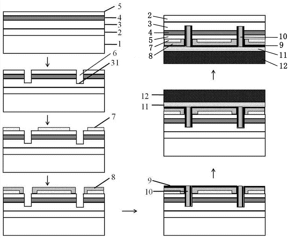
[0034] Such as Figure 2-4 As shown, the embodiment of the present invention provides a method for preparing a GaN-based flip-chip thin-film structure near-ultraviolet LED, including the following steps:

[0035] Step 1) Using a Si substrate as the growth substrate 1, epitaxially growing u-GaN layer 2, n-GaN layer 3, multiple quantum well layer 4 and p-GaN layer 5 on the Si substrate in sequence;

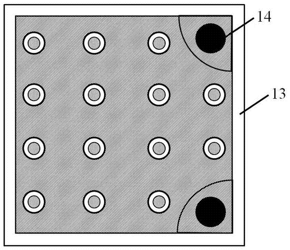
[0036] Step 2) Form a groove 6 that penetrates the p-GaN layer 5 and the multi-quantum well layer 4 and penetrates into the n-GaN layer 3 to a certain depth by photolithography and dry etching in a part of the p-GaN layer 5, exposing the n- GaN surface 31; specifically, the number of etched grooves 6 is 14, that is, the number of exposed n-GaN surfaces 31 is 14;

[0037] Step 3) Fabricate a p-type ohmic contact layer 7 on the surface of the p-GaN layer 5, and the p-type ohmic contact layer also serves as a mirror layer; specifically, the p-type ohmic contact layer 7 is made of ITO,...

Embodiment 2

[0047] This embodiment differs from Embodiment 1 in that:

[0048] Step 1) Using a SiC substrate as a growth substrate 1, epitaxially growing u-GaN layer 2, n-GaN layer 3, multiple quantum well layer 4 and p-GaN layer 5 on the SiC substrate in sequence;

[0049] Step 2) Form a groove 6 that penetrates the p-GaN layer 5 and the multi-quantum well layer 4 and penetrates into the n-GaN layer 3 to a certain depth by photolithography and dry etching in a part of the p-GaN layer 5, exposing the n- GaN surface 31; specifically, the number of etched grooves 6 is one, that is, the number of exposed n-GaN surface 31 is one;

[0050] Step 6) Grow a layer of metal material layer 11 on the insulating layer on the surface of the metal barrier layer 8 and the ohmic contact electrode 10 of n-GaN, and bond the secondary substrate 12 to the metal material layer 11 by means of conductive adhesive bonding superior;

[0051] Step 7) The SiC substrate is removed by grinding combined with ICP etch...

Embodiment 3

[0054] This embodiment differs from Embodiment 1 in that:

[0055] Step 1) Using a sapphire substrate as a growth substrate 1, epitaxially growing u-GaN layer 2, n-GaN layer 3, multiple quantum well layer 4 and p-GaN layer 5 on the sapphire substrate in sequence;

[0056] Step 2) Form a groove 6 that penetrates the p-GaN layer 5 and the multi-quantum well layer 4 and penetrates into the n-GaN layer 3 to a certain depth by photolithography and dry etching in a part of the p-GaN layer 5, exposing the n- GaN surface 31; specifically, the number of etched grooves 6 is 47, that is, the number of exposed n-GaN surfaces 31 is 47;

[0057] Step 6) growing a layer of metal material layer 11 on the insulating layer on the surface of the metal barrier layer 8 and the ohmic contact electrode 10 of n-GaN, and bonding the secondary substrate 12 to the metal material layer 11 by electroplating;

[0058] Step 7) The sapphire substrate is removed by a laser lift-off method to obtain a GaN-bas...


PUM


Abstract

The invention provides a method for preparing a GaN-based inversely-installed thin film structure near-ultraviolet LED. The method comprises the steps of: growing a u-GaN layer, an n-GaN layer, a multi-quantum well layer and a p-GaN layer; forming grooves in the p-GaN layer by means of photolithography and dry etching to expose n-GaN; preparing a p-type ohmic contact layer on the p-GaN layer; preparing a metal barrier layer on the p-type ohmic contact layer; growing an insulating layer on the metal barrier layer and in the grooves, and growing n-GaN ohmic contact electrodes; growing a metal material layer on the insulating layer, and adhering a secondary substrate onto the metal material layer; removing the grown substrate; forming a scribing groove and preparing p welding pads; coarseningu-GaN; and segmenting a chip structure, and completing the preparation of the GaN-based inversely-installed thin film structure near-ultraviolet LED. The method successfully overcomes the technical difficulties of etching process of the u-GaN and N-surface n-GaN ohmic contact, overcomes the electric leakage risk caused by dry grooving and acid grooving, thereby improving the yield and stability of the GaN-based inversely-installed thin film structure near-ultraviolet LED, and is conductive to mass production of chips.

Description

technical field [0001] The invention belongs to the technical field of optoelectronics, and in particular relates to a preparation method of a GaN-based flip-chip thin-film structure near-ultraviolet LED. Background technique [0002] With the continuous deepening of LED research and development, LED technology innovation and application fields continue to expand, and the LED market is becoming wider and wider. Ultraviolet LEDs have gradually entered our field of vision. In the application of the ultraviolet LED market, near-ultraviolet LEDs occupy the largest market share, as high as 90%. Near-ultraviolet LEDs are ideal solid-state light sources to replace mercury-induced ultraviolet light sources due to their long life, low energy consumption, and no pollution. [0003] However, there are still some problems in the application of near-ultraviolet LEDs in the curing exposure market: under a specific curing exposure working distance, near-ultraviolet LEDs with ordinary fron...

Claims


Application Information

Patent Timeline
Patent Type & Authority Applications(China)
IPC IPC(8): H01L33/00H01L33/20
CPCH01L33/0075H01L33/20
Inventor 刘晓燕陈志涛曾昭烩龚政刘久澄任远李叶林
Owner GUANGDONG INST OF SEMICON IND TECH
Why Eureka
Try Eureka