Electrostatic protection circuit and chip having same

A technology for electrostatic protection and circuits, which is used in circuits, electrical components, electrical solid devices, etc.

Inactive Publication Date: 2019-08-06
COSEMITECH SHANGHAI CO LTD
View PDF9 Cites 3 Cited by
  • Summary
  • Abstract
  • Description
  • Claims
  • Application Information

AI Technical Summary

Problems solved by technology

The advantage of this structure is that the protection is relatively sufficient, and the disadvantage is that the normal operating voltage must be guaranteed to be less than the breakdown voltage of the Zener tube

Method used


Image

  • Electrostatic protection circuit and chip having same
  • Electrostatic protection circuit and chip having same
  • Electrostatic protection circuit and chip having same

Examples


Embodiment Construction

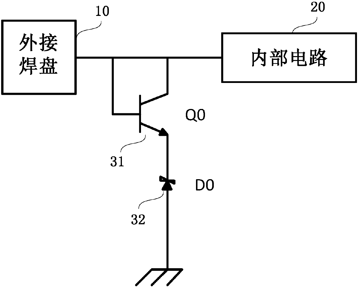
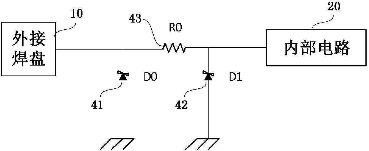
[0031] Example embodiments will now be described more fully with reference to the accompanying drawings. Example embodiments may, however, be embodied in many forms and should not be construed as limited to the embodiments set forth herein. Rather, these embodiments are provided so that this disclosure will be thorough and complete, and will fully convey the concept of the example embodiments to those skilled in the art. The same reference numerals denote the same or similar structures in the drawings, and thus their repeated descriptions will be omitted.

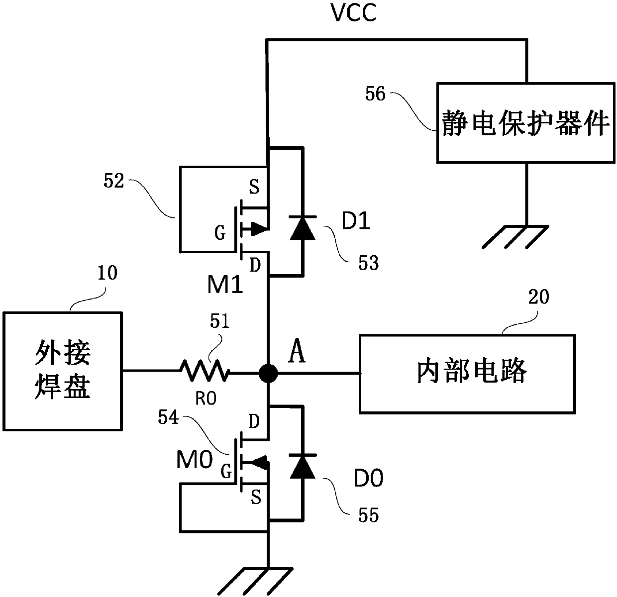
[0032] image 3 It is a schematic diagram of the electrostatic protection circuit of the present invention. Such as image 3 As shown, the electrostatic protection circuit of the present invention includes: an internal circuit 20 and at least one external pad 10 . A resistor 51 , a grounded electrostatic protection device 56 , a P-channel field effect transistor 52 and an N-channel field effect transistor 54 are provide...


PUM


Abstract

The invention provides an electrostatic protection circuit and a chip having the same. The electrostatic protection circuit comprises an internal circuit; an external bonding pad; a resistor connectedin series between the external bonding pad and the internal circuit; a grounded electrostatic protection device; a P-channel field effect transistor the source of which is connected to the gate and the electrostatic protection device, the drain of which is connected to a node between the resistor and the internal circuit, and the source and the drain of which has a first parasitic diode therebetween that forms a first electrostatic discharge circuit with the electrostatic protection device; and an N-channel field effect transistor the source of which is connected to the gate and the ground, the drain of the which is connected to a node between the resistor and the internal circuit, and the second parasitic diode of which forms a second electrostatic discharge circuit. The electrostatic protection circuit achieves good electrostatic protection, saves chip area and improves reliability.

Description

technical field [0001] The invention relates to the field of electrostatic protection, in particular to an electrostatic protection circuit and a chip with the electrostatic protection circuit. Background technique [0002] Any friction can generate static electricity, for example: in dry weather, scratching across the carpet, and then touching the metal doorknob, visible sparks will be transferred from the finger to the doorknob. The human body can be equivalent to a capacitor, and it can be regarded as charging the capacitor when it is drawn across the carpet, which can reach 10000V or higher. When a finger is near the doorknob, the sudden discharge can cause visible sparks and a felt shock. For a CMOS device of an integrated circuit, a discharge lower than 50V can destroy the gate oxide dielectric layer of the device. [0003] Electrostatic discharge may also cause damage to the dielectric layer; degradation of the performance of the dielectric layer; avalanche breakdow...

Claims


Application Information

Patent Timeline
Patent Type & Authority Applications(China)
IPC IPC(8): H01L27/02
CPCH01L27/0248H01L27/0266
Inventor 尹小平游剑
Owner COSEMITECH SHANGHAI CO LTD
Why Eureka
Try Eureka