Display substrate, preparation method thereof, and display device

A technology for displaying substrates and display areas, which is applied in semiconductor/solid-state device manufacturing, semiconductor devices, electrical components, etc., and can solve problems such as package failure

Active Publication Date: 2019-08-13
BOE TECH GRP CO LTD +1
View PDF5 Cites 20 Cited by
  • Summary
  • Abstract
  • Description
  • Claims
  • Application Information

AI Technical Summary

Problems solved by technology

[0005] The technical problem to be solved by the embodiments of the present invention is to provide a display substrate and it

Method used


Image

  • Display substrate, preparation method thereof, and display device
  • Display substrate, preparation method thereof, and display device
  • Display substrate, preparation method thereof, and display device

Examples


no. 1 example

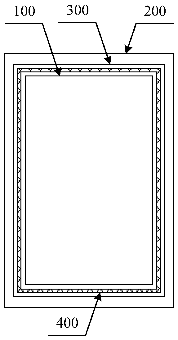
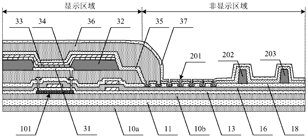
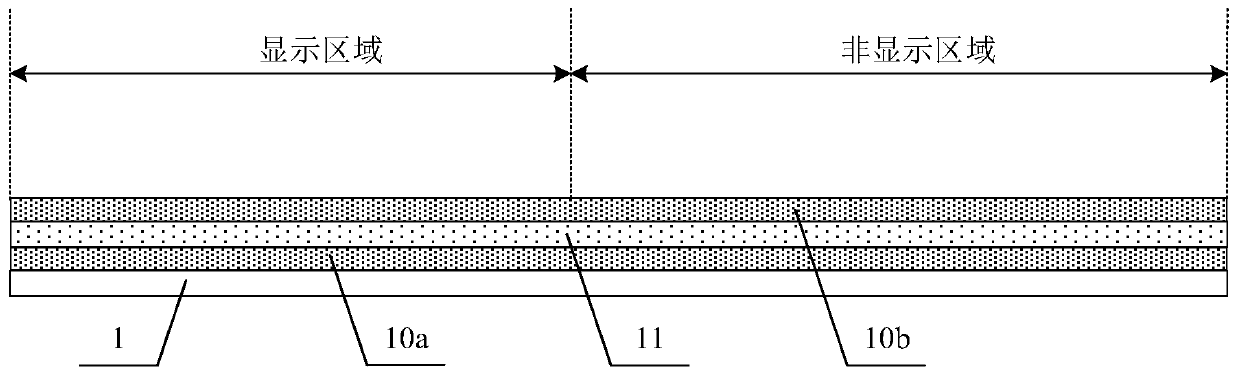
[0060] figure 2 It is a schematic structural diagram of the first embodiment of the display substrate of the present invention, showing the structure of the display area and the non-display area on a plane perpendicular to the display substrate. like figure 2 As shown, on a plane perpendicular to the display substrate, the main structure of the display area includes a driving structure layer and a light emitting structure layer arranged on the substrate, and the driving structure layer includes a plurality of thin film transistors, figure 2 Only one light emitting unit and one thin film transistor are taken as examples for illustration. Specifically, the substrate includes a first substrate 10a, a buffer layer 11 disposed on the first substrate 10a, and a second substrate 10b disposed on the buffer layer 11, and the driving structure layer mainly includes a thin film transistor 101 disposed on the second substrate 10b. . The light emitting structure layer mainly includes...

no. 2 example

[0083] Figure 12 It is a schematic structural diagram of the second embodiment of the display substrate of the present invention, illustrating the structure of the display area and the non-display area on a plane perpendicular to the display substrate. The main structure of the display substrate in this embodiment is basically the same as that of the aforementioned first embodiment. The main structure of the display area includes a plurality of light-emitting units distributed in an array, and each light-emitting unit includes a driving structure layer and a light-emitting structure layer arranged on the substrate. The main structure of the non-display area includes an insulating layer arranged on the base, a retaining wall arranged on the insulating layer, an inorganic packaging layer covering the retaining wall, and a strengthening structure. like Figure 12 As shown, different from the aforementioned first embodiment, the reinforcing structure of this embodiment is arrang...

no. 3 example

[0089] Based on the technical idea of ​​the embodiment of the present invention, the embodiment of the present invention also provides a method for preparing a display substrate. The display substrate includes a display area and a non-display area, and the preparation method of the display substrate in this embodiment includes:

[0090] S1. Forming a functional layer in the non-display area, the functional layer comprising a plurality of grooves arranged at intervals;

[0091] S2. Form a retaining wall in the non-display area, so that the plurality of grooves arranged at intervals are located between the display area and the retaining wall;

[0092] S3, forming an inorganic encapsulation layer covering the functional layer and the retaining wall in the non-display area, so that a contact surface between the functional layer and the inorganic encapsulation layer forms a concave-convex structure.

[0093] In one embodiment, step S1 comprises:

[0094] form the base;

[0095] ...


PUM


Abstract

The invention provides a display substrate, a preparation method thereof, and a display device. The display substrate comprises a display area and a non-display area. The non-display area comprises afunctional layer, a retaining wall arranged on the functional layer, and an inorganic packaging layer covering the functional layer and the retaining wall. Between the display area and the retaining wall, the functional layer comprises a plurality of grooves arranged at intervals, so that a concave-convex structure is formed on the contact surface of the functional layer and the inorganic packaging layer. According to the invention, the plurality of grooves are formed in the area between the display area and the retaining wall at intervals, so a concave-convex structure is formed on the contact surface of the functional layer and the inorganic packaging layer, thereby increasing the bonding force of the film layer in the area, avoiding the delamination or cracking of an area between the display area and the retaining wall, avoiding a water and oxygen invasion path formed by delamination or cracking, and effectively guaranteeing the effectiveness and reliability of packaging. Moreover,the display substrate is low in manufacturing cost, is easy in process implementation and the like.

Description

technical field [0001] The invention relates to the field of display technology, in particular to a display substrate, a preparation method thereof, and a display device. Background technique [0002] Organic Light Emitting Diode (OLED) is an active light-emitting display device, which has the advantages of self-illumination, wide viewing angle, high contrast, low power consumption, fast response, bright colors, thin and bendable, etc. With the continuous development of display technology, OLED technology is more and more applied to various display devices, and has become the mainstream in the current market. [0003] Because OLED display technology uses organic light-emitting materials to emit light, organic light-emitting materials are easy to react with water and oxygen, and a small amount of water vapor and oxygen can damage organic light-emitting materials and deteriorate the light-emitting performance of OLED panels. Therefore, OLED panels have a very high impact on pa...

Claims


Application Information

Patent Timeline
IPC IPC(8): H01L51/52H01L51/56
CPCH10K50/84H10K71/00
Inventor 宋丽蒋志亮
Owner BOE TECH GRP CO LTD
Why Eureka
Try Eureka