mram chip

A chip and bit line technology, applied in the field of MRAM chips, can solve problems such as insufficient SL source line width, and achieve the effects of simple design, reduced energy consumption, and reduced cost

Active Publication Date: 2021-03-23
SHANGHAI CIYU INFORMATION TECH CO LTD
View PDF13 Cites 0 Cited by
  • Summary
  • Abstract
  • Description
  • Claims
  • Application Information

AI Technical Summary

Problems solved by technology

In the design, it is often difficult due to the insufficient width of the SL source line

Method used


Image

  • mram chip
  • mram chip
  • mram chip

Examples


Embodiment Construction

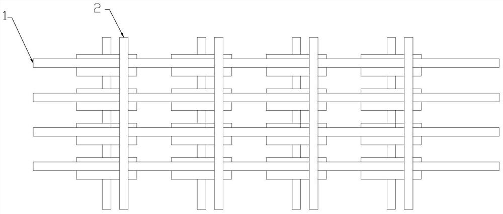
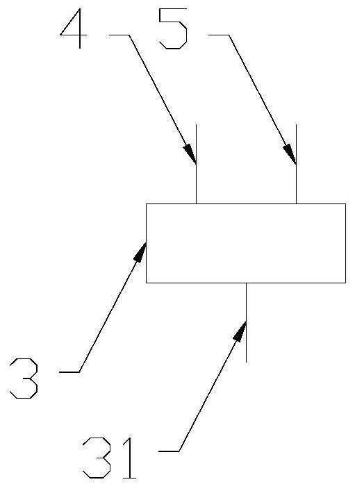
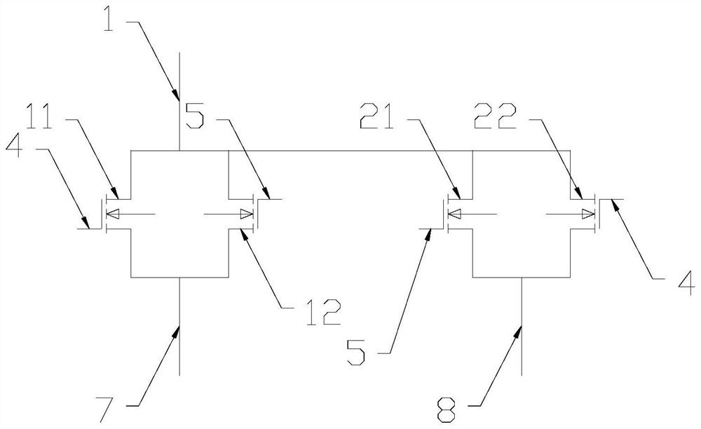
[0020] as the picture shows, figure 1 is the circuit diagram of the precoder of the present invention, figure 2 It is the circuit diagram of the pre-decoder of the present invention, a kind of MRAM chip, comprising: the MRAM array and the pre-decoder 3 of vertical layout of source line 2 and bit line 1, source line 2 (SL) and bit line 1 (BL) of MRAM array Vertical layout, a common bit line 7 is connected to a plurality of bit lines 1, wherein the MRAM array includes a plurality of sub-arrays, and the sub-array includes a common source line 8 connected to all cells, and the common source line 8 is connected to a plurality of bit lines 1 in each column Specifically, every n columns can be used as a group, and the sub-array includes a common source line 8 connected to multiple source lines 2, and the SLs of all rows in each group are connected together through a common SL; each bit line 1 Connect the first transmission gate and the second transmission gate; the first transmissi...


PUM


Abstract

The invention discloses an MRAM chip, in which an MRAM array comprises a plurality of sub-arrays, wherein each sub-array comprises a common source line connected to all cells and a plurality of bit lines connected to each column; each bit line is connected with a first transmission gate and a second transmission gate; the first transmission gate is connected with the common source line, and the second transmission gate is connected with the common bit line; a pre-decoder comprises input of a plurality of address line, and output of selection signals matching the number of the bit lines and inverted signals of the selection signals; and the output end of the selection signals and the inverted signals is connected to the first transmission gate and the second transmission gate correspondingto the corresponding bit line of each sub-array to control any one of the first transmission gate and the second transmission gate to be opened and the other one to be closed. Through the control of the pre-decoder, only one bit is written in one array each time, and high voltage and negative voltage are not needed any more, and the design is simple, and the energy consumption is reduced.

Description

technical field [0001] The invention relates to a semiconductor chip, in particular to an MRAM chip. Background technique [0002] MRAM is a new memory and storage technology that can be read and written as fast as SRAM / DRAM, and can permanently retain data after power failure like Flash memory. [0003] Its economy is ideally good, and the silicon chip area occupied per unit capacity has a great advantage over SRAM, and also has advantages over NOR Flash, which is often used in such chips, and has greater advantages than embedded NOR Flash. Its performance is also quite good, the read and write latency is close to the best SRAM, and the power consumption is the best among various memory and storage technologies. Moreover, MRAM is not compatible with standard CMOS semiconductor processes like DRAM and Flash. MRAM can be integrated into a chip with logic circuits. [0004] The principle of MRAM is based on a structure called MTJ (magnetic tunnel junction). It consists of ...

Claims


Application Information

Patent Timeline
Patent Type & Authority Patents(China)
IPC IPC(8): G11C11/16
CPCG11C11/1653G11C11/1655
Inventor 戴瑾
Owner SHANGHAI CIYU INFORMATION TECH CO LTD
Why Eureka
Try Eureka