Small-spacing close-packed vertical cavity surface emitting laser and preparation method thereof
A vertical cavity surface emission, small spacing technology, applied in the field of lasers, can solve the problems of wafer surface warpage, unfavorable laser high-precision lithography, etc., to reduce the warpage degree and improve the lithography accuracy.
- Summary
- Abstract
- Description
- Claims
- Application Information
AI Technical Summary
Problems solved by technology
Method used
Image
Examples
preparation example Construction
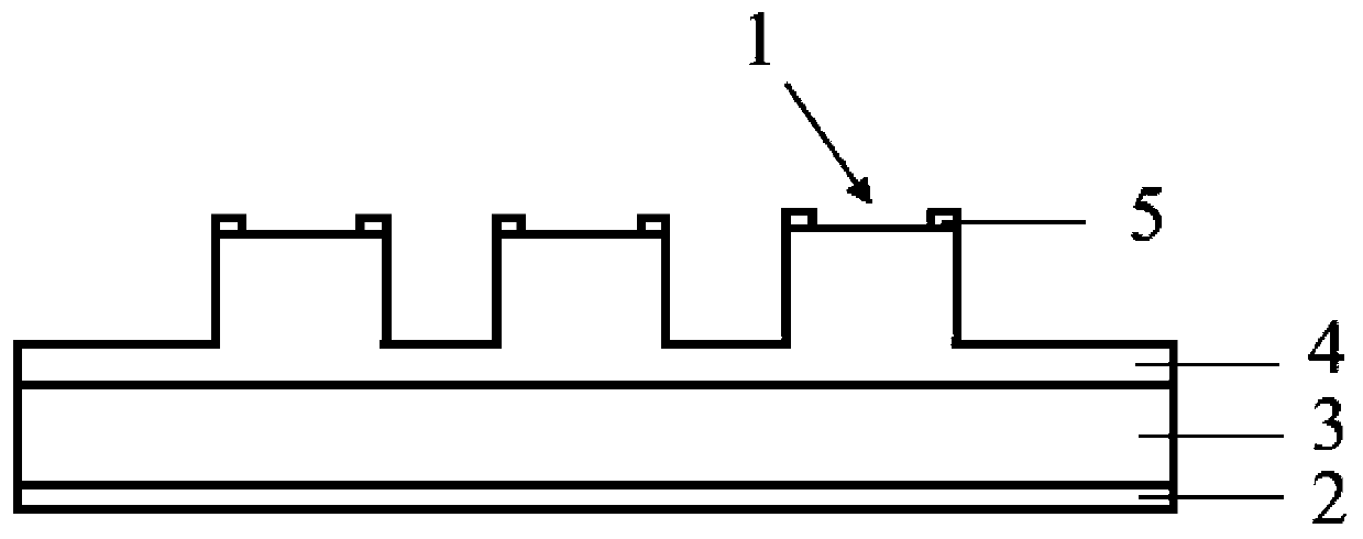
[0042] Based on the above-mentioned small-pitch emitting laser, the present invention also provides a preparation method of the above-mentioned small-pitch emitting laser, which includes the following steps:
[0043] S1. An epitaxial layer is grown on the upper surface of the substrate by an epitaxial process.
[0044] S2. Growing a dielectric layer on the lower surface of the substrate to reduce chip warpage.
[0045] Preferably, the dielectric layer is one or more of silicon oxide, silicon nitride, and aluminum oxide. By growing the dielectric layer, it is beneficial to balance the internal stress of the laser chip, flatten the surface of the laser chip, and remove the warpage of the laser chip surface, thereby improving the lithography precision and realizing the small-pitch arrangement of Mesa mesa in the etching process.
[0046] S3. Defining electrode patterns on the upper surface of the epitaxial layer, and forming electrodes after electron beam deposition and electrod...
PUM
 Abstract
Description
Claims
Application Information


