A small-pitch close-packed vertical-cavity surface-emitting laser and its preparation method

A vertical-cavity surface-emitting, small-pitch technology, applied in the field of lasers, can solve problems such as unfavorable laser high-precision lithography, wafer surface warpage, etc., and achieve the effect of improving lithography accuracy and reducing warpage

Active Publication Date: 2020-09-25
EVERBRIGHT INST OF SEMICON PHOTONICS CO LTD
View PDF5 Cites 0 Cited by
  • Summary
  • Abstract
  • Description
  • Claims
  • Application Information

AI Technical Summary

Problems solved by technology

[0003] The difficulty in manufacturing small-pitch close-packed vertical-cavity surface-emitting lasers mainly comes from the warping of the wafer surface after the substrate is grown epitaxially, which is not conducive to the realization of high-precision lithography of small-pitch close-packed vertical-cavity surface-emitting lasers.

Method used


Image

  • A small-pitch close-packed vertical-cavity surface-emitting laser and its preparation method
  • A small-pitch close-packed vertical-cavity surface-emitting laser and its preparation method
  • A small-pitch close-packed vertical-cavity surface-emitting laser and its preparation method

Examples


preparation example Construction

[0042] Based on the above-mentioned small-pitch emitting laser, the present invention also provides a preparation method of the above-mentioned small-pitch emitting laser, which includes the following steps:

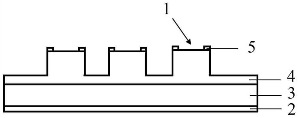
[0043] S1. An epitaxial layer is grown on the upper surface of the substrate by an epitaxial process.

[0044] S2. Growing a dielectric layer on the lower surface of the substrate to reduce chip warpage.

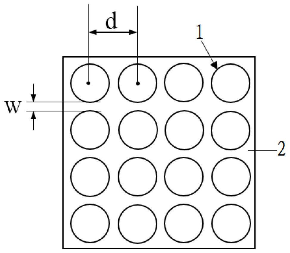
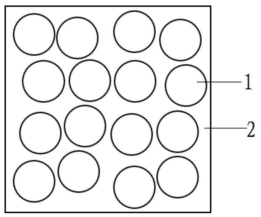
[0045] Preferably, the dielectric layer is one or more of silicon oxide, silicon nitride, and aluminum oxide. By growing the dielectric layer, it is beneficial to balance the internal stress of the laser chip, flatten the surface of the laser chip, and remove the warpage of the laser chip surface, thereby improving the lithography precision and realizing the small-pitch arrangement of Mesa mesa in the etching process.

[0046] S3. Defining electrode patterns on the upper surface of the epitaxial layer, and forming electrodes after electron beam deposition and electrod...


PUM

PropertyMeasurementUnit
thicknessaaaaaaaaaa
thicknessaaaaaaaaaa
thicknessaaaaaaaaaa

Abstract

The invention provides a small-spacing close-packed vertical cavity surface emitting laser and a preparation method thereof. The laser includes a substrate, an epitaxial layer, mesas prepared on the epitaxial layer, upper electrodes and a lower electrode. The multiple mesas are arranged on the surface of one side of the epitaxial layer. Any mesa forms a light emitting point of the epitaxial layer.Any mesa is provided with upper electrodes thereon. The lower electrode is arranged on the surface of one side of the substrate. The center spacing between adjacent mesas is 8-20 microns, and the edge spacing between adjacent mesas is 0.5-5 microns. A layer of silicon oxide, silicon nitride or other dielectric material is deposited on the back of the epitaxial wafer. By adjusting the thickness and stress level of the material, the warpage of the epitaxial wafer is reduced. Therefore, the lithography precision in the manufacture of the small-spacing close-packed vertical cavity surface emitting laser is improved, and the preparation of a small-spacing close-packed vertical cavity surface emitting laser is realized.

Description

technical field [0001] The invention relates to the technical field of lasers, in particular to a small-pitch close-packed vertical-cavity surface-emitting laser and a preparation method thereof. Background technique [0002] With the development of technologies and applications such as 3D face recognition and lidar, vertical cavity surface emitting lasers (VCSELs) have attracted more and more attention. In order to continuously improve the imaging accuracy and luminous power of VCSEL arrays, researchers have continuously improved the design and process level of VCSEL devices, and have made some progress. Among various methods, increasing the light-emitting point density of vertical cavity surface lasers and preparing small-pitch close-packed vertical cavity surface emitting lasers is an important method to improve the imaging resolution and luminous power of VCSEL devices. [0003] The difficulty in the fabrication of small-pitch vertical-cavity surface-emitting lasers is ...

Claims


Application Information

Patent Timeline
Patent Type & Authority Patents(China)
IPC IPC(8): H01S5/183H01S5/042H01S5/187
CPCH01S5/0425H01S5/18344H01S5/187
Inventor 王俊刘恒谭少阳荣宇峰
Owner EVERBRIGHT INST OF SEMICON PHOTONICS CO LTD
Why Eureka
Try Eureka