A vertical cavity surface emitting laser and its manufacturing method

A vertical cavity surface emission and laser technology, applied in the field of lasers, can solve the problems of uneven VCSEL power and adverse effects on crystal quality, and achieve the effect of improving power uniformity and good crystal quality

Active Publication Date: 2021-04-20
YANGZHOU CHANGELIGHT
View PDF4 Cites 0 Cited by
  • Summary
  • Abstract
  • Description
  • Claims
  • Application Information

AI Technical Summary

Problems solved by technology

[0004] However, in the prior art, since there are a large number of defects inside and on the surface of the gallium arsenide substrate itself, these defects will adversely affect the crystal quality of the epitaxial structure grown on the surface of the gallium arsenide substrate, thereby making the power of the VCSEL uneven

Method used


Image

  • A vertical cavity surface emitting laser and its manufacturing method
  • A vertical cavity surface emitting laser and its manufacturing method
  • A vertical cavity surface emitting laser and its manufacturing method

Examples


preparation example Construction

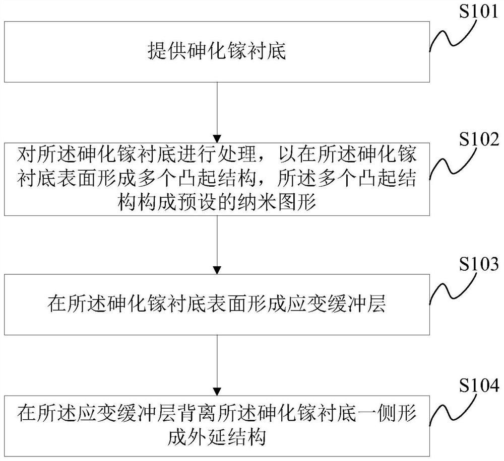
[0047] The embodiment of the present application provides a preparation method of a vertical cavity surface emitting laser, such as figure 1 shown, including:

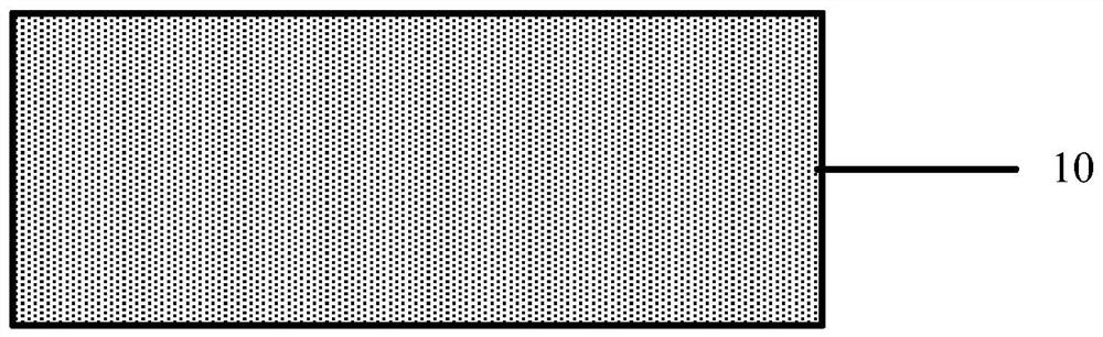
[0048] S101: providing a gallium arsenide substrate;

[0049] Such as figure 2 as shown, figure 2 shows a schematic cross-sectional view of the gallium arsenide substrate provided in step S101; figure 2 The number 10 in represents the gallium arsenide substrate;

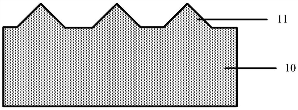
[0050] S102: Processing the gallium arsenide substrate to form a plurality of raised structures on the surface of the gallium arsenide substrate, the plurality of raised structures forming a preset nano-pattern;

[0051] refer to image 3 , image 3 A schematic cross-sectional structure diagram showing the gallium arsenide substrate and its surface structure after step S102; image 3 The number 11 in represents the raised structure.

[0052] S103: forming a strain buffer layer on the surface of the gallium arsenide substrate;

[0053] refer to F...


PUM


Abstract

The present application discloses a vertical cavity surface emitting laser and a manufacturing method thereof, wherein, the manufacturing method of the vertical cavity surface emitting laser forms a plurality of convex structures constituting preset nano-patterns on the surface of a gallium arsenide substrate , and a strain buffer layer is formed on the surface of one side with the raised structure to provide a good foundation for the growth of the epitaxial structure; wherein, the plurality of raised structures provide the bending in the growth direction of the defect density in the gallium arsenide substrate Basically, the strain buffer layer provides a flat epitaxial structure growth surface, so that the epitaxial structure grown on the surface of the strain buffer layer can avoid the adverse effects of defects in the gallium arsenide substrate to the greatest extent, so that the epitaxial structure grown on the strain buffer layer The epitaxial structure on the surface can have good crystal quality, which improves the power uniformity of the vertical cavity surface emitting laser.

Description

technical field [0001] The present application relates to the technical field of lasers, and more specifically, to a vertical cavity surface emitting laser and a preparation method thereof. Background technique [0002] A vertical cavity surface emitting laser (Vertical Cavity Surface Emitting Laser, VCSEL) is a laser made of gallium arsenide semiconductor material. [0003] VCSEL is different from other light sources such as light emitting diode (Light Emitting Diode, LED) and laser diode (Laserdiode, LD). VCSEL has small size, circular output spot, single longitudinal mode output, small threshold current, low price and easy integration The advantages of large-area arrays are widely used in optical communication, optical interconnection, optical storage and other fields. [0004] However, in the prior art, since there are a large number of defects inside and on the surface of the gallium arsenide substrate itself, these defects will adversely affect the crystal quality of ...

Claims


Application Information

Patent Timeline
Patent Type & Authority Patents(China)
IPC IPC(8): H01S5/183H01S5/22
CPCH01S5/18305H01S5/2207
Inventor 杜石磊田宇韩效亚吴真龙
Owner YANGZHOU CHANGELIGHT
Why Eureka
Try Eureka