Organic light emitting diode display device and manufacturing method thereof

A technology of light-emitting diodes and display devices, applied in semiconductor/solid-state device manufacturing, electrical components, electric solid-state devices, etc., can solve problems such as large uncontrollability, increased energy consumption, dark brightness in the central area of ​​the screen, etc., to avoid unavoidable The effect of controlling factors, ensuring flatness, and improving yield

A technology of light-emitting diodes and display devices, applied in semiconductor/solid-state device manufacturing, electrical components, electric solid-state devices, etc., can solve problems such as large uncontrollability, increased energy consumption, dark brightness in the central area of ​​the screen, etc., to avoid unavoidable The effect of controlling factors, ensuring flatness, and improving yield

CN110176478AInactive Publication Date: 2019-08-27SHENZHEN CHINA STAR OPTOELECTRONICS SEMICON DISPLAY TECH CO LTD

Image

  • Organic light emitting diode display device and manufacturing method thereof
  • Organic light emitting diode display device and manufacturing method thereof
  • Organic light emitting diode display device and manufacturing method thereof

Examples


Embodiment Construction

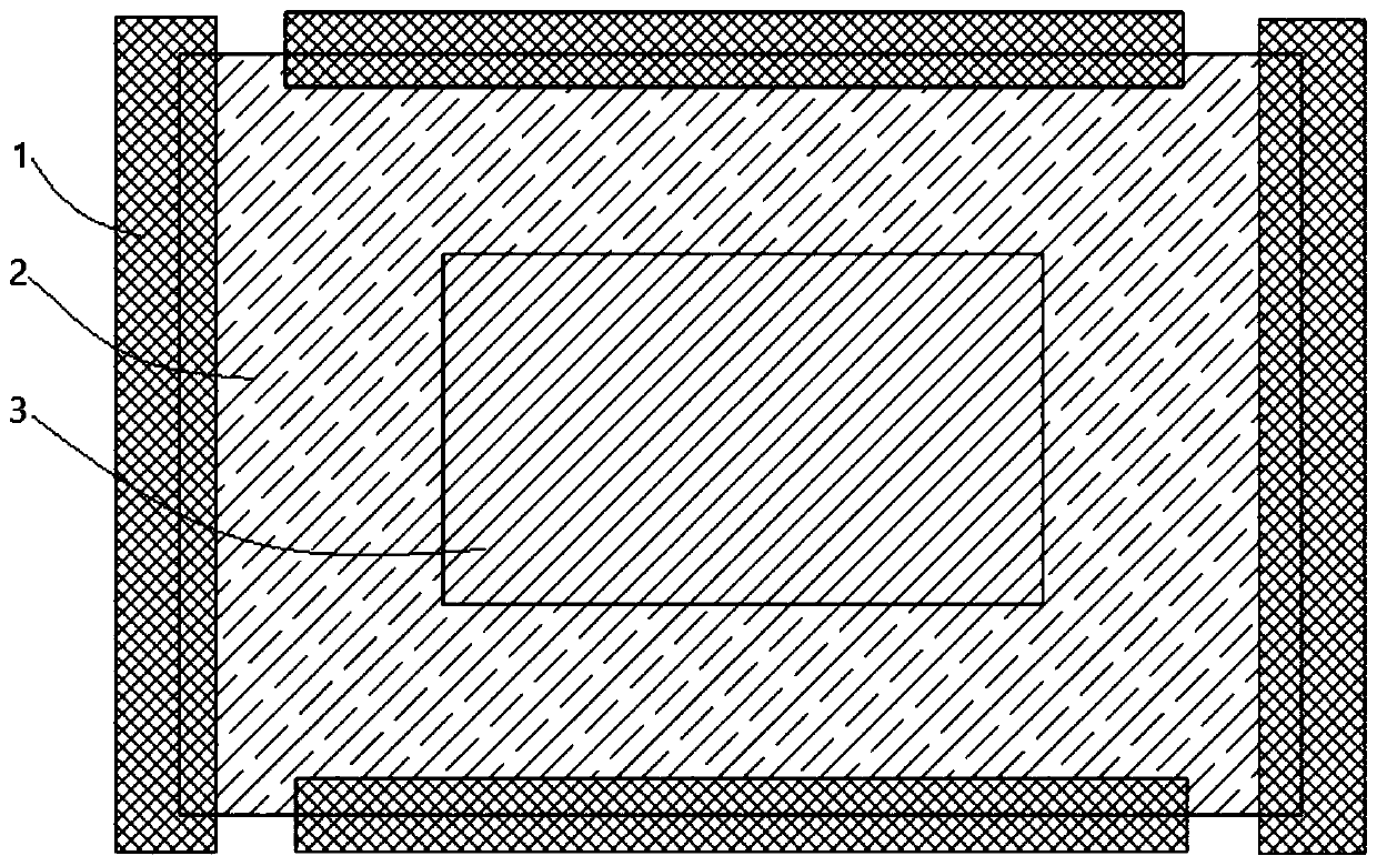
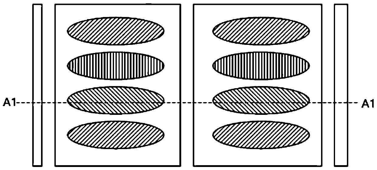
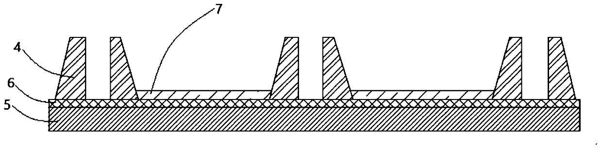
[0032] The technical solutions in the embodiments of the present invention will be clearly and completely described below in conjunction with the accompanying drawings in the embodiments of the present invention. Obviously, the described embodiments are only some of the embodiments of the present invention, not all of them. Based on The embodiments of the present invention, and all other embodiments obtained by those skilled in the art without creative work, all belong to the protection scope of the present invention.

[0033] In describing the present invention, it should be understood that the terms "center", "longitudinal", "transverse", "length", "width", "thickness", "upper", "lower", "front", " Orientation indicated by rear, left, right, vertical, horizontal, top, bottom, inside, outside, clockwise, counterclockwise, etc. The positional relationship is based on the orientation or positional relationship shown in the drawings, which is only for the convenience of describi...


PUM


Abstract

The present invention discloses an organic light emitting diode display device and a manufacturing method thereof. The organic light emitting diode display device comprises a base plate comprising a substrate. A thin film transistor circuit layer is arranged on the substrate and has a control circuit; at least one groove is provided on the thin film transistor circuit layer; the bottom of the groove is provided with an electron transport layer; and at least one groove is filled with an auxiliary cathode layer. An anode layer is arranged on the thin film transistor circuit layer; a luminescentlayer is uniformly arranged on the anode layer; and the electron transport layer is also arranged on the luminescent layer. The cathode layer covers the electron transport layer and the auxiliary cathode layer, thereby the complexity of the thin film transistor circuit layer is avoided; the flatness of the pixel surface is ensured and the product yield is improved.

Description

technical field [0001] The invention relates to the field of display panels, in particular to an organic light emitting diode display device and a manufacturing method thereof. Background technique [0002] Organic Light-Emitting Diode (OLED) has become the most promising new display device in recent years due to its advantages of self-luminescence, all-solid-state, high contrast, etc. [0003] At present, the application direction of OLED includes RGB OLED technology composed of red (Red, R), green (Green, G), blue (Blue, B) and other three primary color pixels (pixels) arranged side by side (Side by Side), and white light OLED (WhiteOLED) plus color filter (Color Filter, CF) technology two categories. The products are mainly divided into small-sized mobile phones, tablet computer (Pad) screens and larger-sized TV (Television, TV) screens. [0004] In the direction of large-size OLED applications, the products currently on the market are concentrated in the bottom (Bottom...

Claims


Application Information

Patent Timeline
27 Aug 2019
Publication
CN110176478A
IPC
H01L27/32; H01L51/50; H01L51/52; H01L51/56; H01L27/12
CPC
H01L27/124; H10K59/35; H10K59/123; H10K59/131; H10K50/16; H10K50/824; H10K50/11; H10K71/00
Inventors
郝鹏