White-light LED structure with extremely high barrier layer insertion layer

A technology of LED structure and insertion layer, which is applied in the direction of electrical components, circuits, semiconductor devices, etc., can solve the problems of high production cost and complicated production process, and achieve the effect of reducing packaging process and reducing stability problems

Pending Publication Date: 2019-08-27
江西乾照光电有限公司
View PDF3 Cites 2 Cited by
  • Summary
  • Abstract
  • Description
  • Claims
  • Application Information

AI Technical Summary

Problems solved by technology

[0005] Among them, the first method, phosphor-converted white LED, is the most commonly used method, but the loss of light efficiency due to white light frequency reduction is 10%-30%. In addition, there are stability problems of phosphor aging and packaging cost problems, and Dependency issues on GaN-based LEDs
The production process of the second method is more complicated, and the production cost is high

Method used


Image

  • White-light LED structure with extremely high barrier layer insertion layer
  • White-light LED structure with extremely high barrier layer insertion layer
  • White-light LED structure with extremely high barrier layer insertion layer

Examples


Embodiment 1

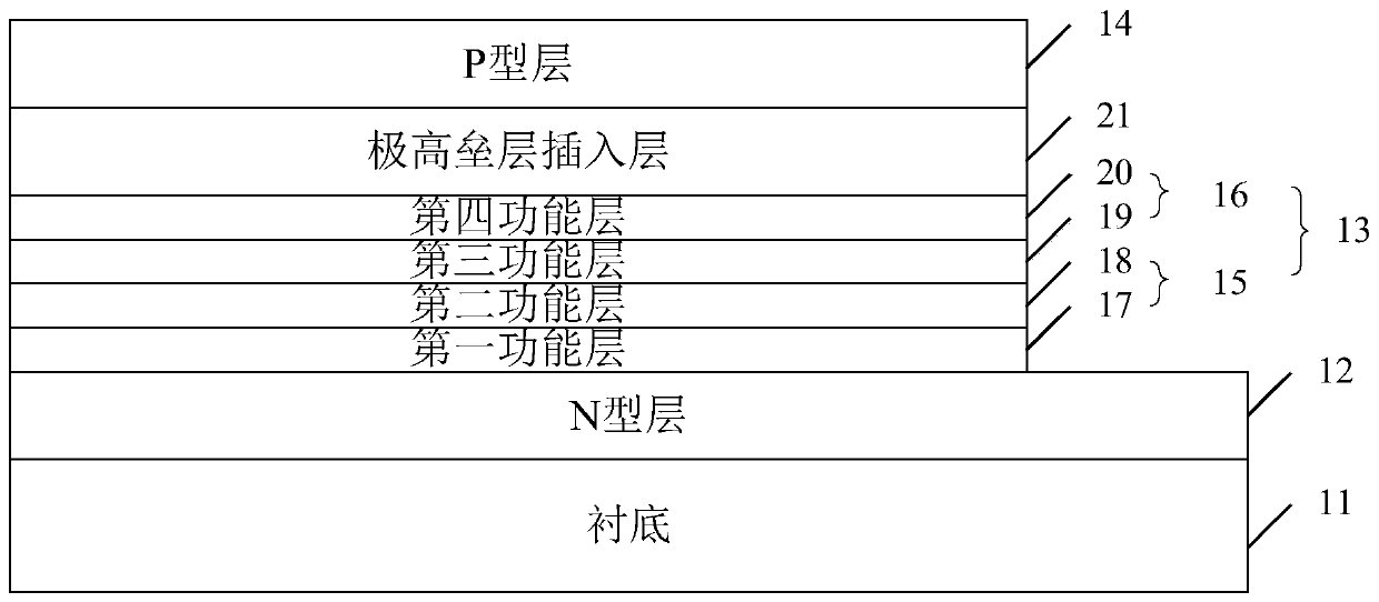
[0087] refer to figure 2 , figure 2 A schematic structural diagram of another white light LED structure with an extremely high barrier insertion layer provided by an embodiment of the present invention.

[0088] Step 1: Using equipment MOCVD, trimethylgallium TMGa, triethylgallium TEGa, ammonia NH 3 Ga source, N source, N 2 is the carrier gas, the N-type and P-type dopant sources are silane SiH respectively 4 and Magnesium CP 2 Mg, use InGaN ternary substrate, In composition is 0.1.

[0089] Step 2: Put the InGaN substrate 11 into the MOCVD reaction chamber, pass through TMGa, TMIn, SIH 4 , NH 3 N-type layer 12 is grown, and the concentration of Si is 6×10 18 / cm 3 , the In component is 0.1; the thickness is 0.5 μm.

[0090] Step 3: Introduce TEGa, TMIn, NH 3 The first functional layer 17 is grown with a thickness of 4 nm and an In composition of 0.35.

[0091] Step 4: Introduce TEGa, TMIn, NH 3 Grow the second functional layer 18, thickness 6nm, In composition 0...

Embodiment 2

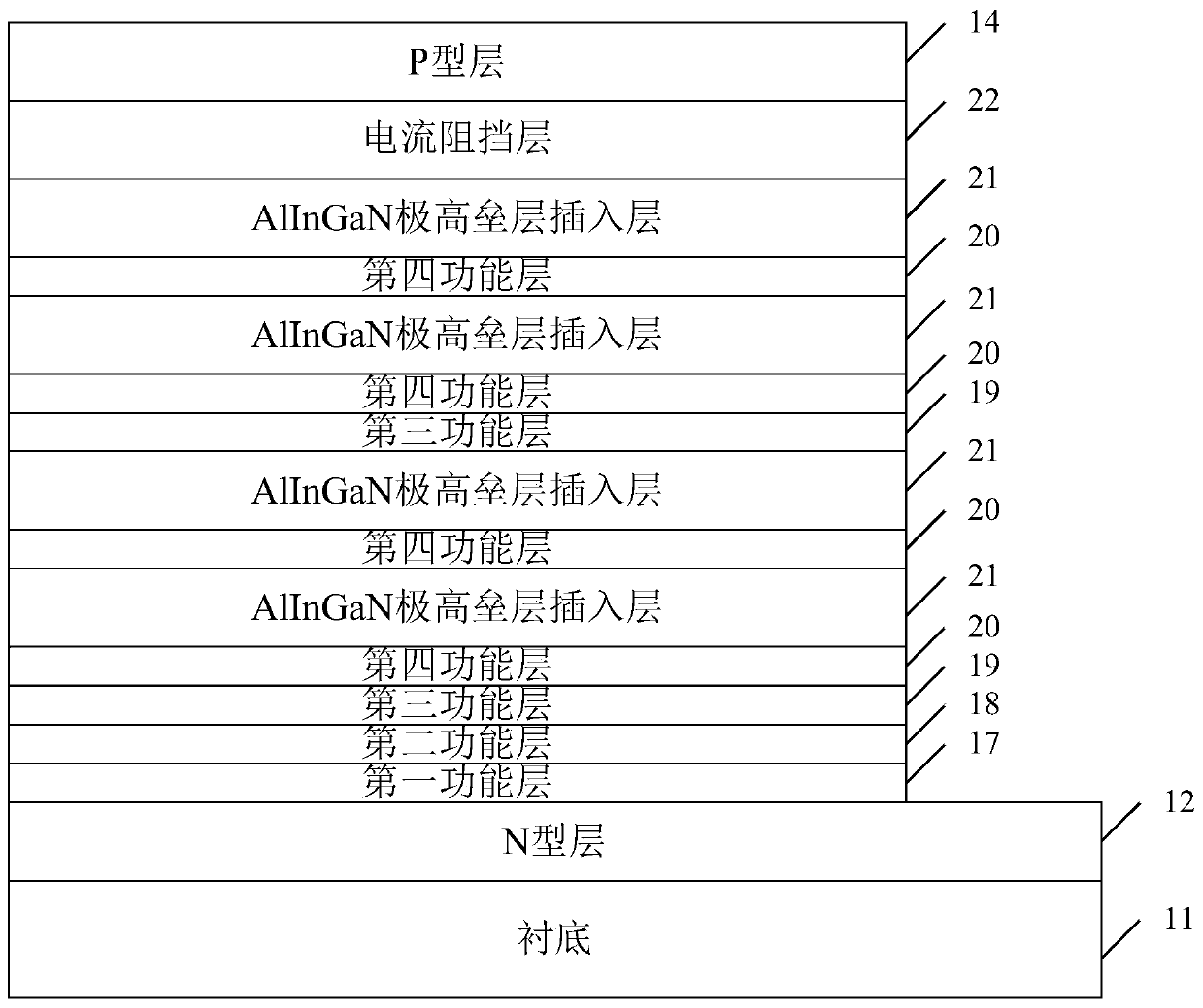
[0103] refer to image 3 , image 3 A schematic structural diagram of yet another white light LED structure with a very high barrier insertion layer provided by an embodiment of the present invention.

[0104] Step 1: Using equipment MOCVD, trimethylgallium TMGa, triethylgallium TEGa, ammonia NH 3 Ga source, N source, N 2 is the carrier gas, the N-type and P-type dopant sources are silane SiH respectively 4 and Magnesium CP 2 Mg, use InGaN ternary substrate, In composition is 0.1.

[0105] Step 2: Put the InGaN substrate 11 into the MOCVD reaction chamber, and feed TMGa, TMIn, SIH4, NH 3 N-type layer 12 is grown, and the concentration of Si is 6×10 18 / cm 3 , the In component is 0.1; the thickness is 0.5 μm.

[0106] Step 3: Introduce TEGa, TMIn, NH 3 The first functional layer 17 is grown with a thickness of 4 nm and an In composition of 0.35.

[0107] Step 4: Introduce TEGa, TMIn, NH 3 Grow the second functional layer 18, thickness 6nm, In composition 0.1, SiH 4 ...

Embodiment 3

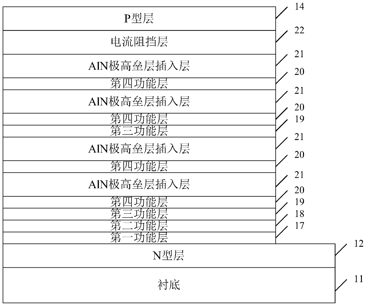
[0120] refer to Figure 4 , Figure 4 A schematic structural diagram of yet another white light LED structure with a very high barrier insertion layer provided by an embodiment of the present invention.

[0121] Step 1: Using equipment MOCVD, trimethylgallium TMGa, triethylgallium TEGa, ammonia NH 3 Ga source, N source, N 2 is the carrier gas, the N-type and P-type dopant sources are silane SiH respectively 4 and Magnesium CP 2 Mg, use InGaN ternary substrate, In composition is 0.1.

[0122] Step 2: Put the InGaN substrate 11 into the MOCVD reaction chamber, pass through TMGa, TMIn, SIH 4 , NH 3 N-type layer 12 is grown, and the concentration of Si is 6×10 18 / cm 3 , the In component is 0.1; the thickness is 0.5 μm.

[0123] Step 3: Introduce TEGa, TMIn, NH 3 The first functional layer 17 is grown with a thickness of 4 nm and an In composition of 0.35.

[0124] Step 4: Introduce TEGa, TMIn, NH 3 Grow the second functional layer 18, thickness 6nm, In composition 0.1...


PUM


Abstract

The invention provides a white-light LED structure with an extremely high barrier layer insertion layer. In the white-light LED structure with the extremely high barrier layer insertion layer, a dual-band MQW layer is grown on a substrate, so that the white-light LED structure is used for simultaneously stimulating blue light and yellow light, and the blue light and the yellow light are mixed to generate white light; and with the structure of inserting the extremely high barrier layer insertion layer into the blue-band MQW layer, the problem of energy band of a blue light-emitting region to cause that blue-light spectrum cannot be simulated can be prevented, and white-light LED with high light-emitting efficiency, good stability and uniform chromaticity is further successfully grown. Compared with an existing white-light LED technology, fluorescent powder is not used, thus, the package process can be reduced, and the problem of stability generated by fluorescent powder aging also can be reduced.

Description

technical field [0001] The invention relates to the technical field of LEDs, and more specifically relates to a white LED structure with a very high barrier insertion layer. Background technique [0002] The wavelength range of the visible light spectrum is 380nm-760nm, which is the seven-color light that can be felt by the human eye, namely red, orange, yellow, green, blue, blue, and purple, but the seven-color light is a kind of monochromatic light. It is not monochromatic light, so there is no white light in the spectrum of visible light, it is composite light synthesized from multiple monochromatic lights. [0003] Then, to make the LED emit white light, its spectral characteristics should include the entire visible spectral range. According to research on visible light, white light that can be seen by the human eye requires at least a mixture of two kinds of light, that is, two-wavelength light emission (blue light + yellow light) or three-wavelength light emission (bl...

Claims


Application Information

Patent Timeline
Patent Type & Authority Applications(China)
IPC IPC(8): H01L33/20H01L33/50
CPCH01L33/504H01L33/20
Inventor 霍丽艳滕龙刘锐森崔晓慧林加城周浩方誉谢祥彬刘兆
Owner 江西乾照光电有限公司
Why Eureka
Try Eureka