Visible light broadband perfect absorber based on semiconductor metasurface

A visible light and metasurface technology, applied in the optical field, can solve the problems of narrow absorption bandwidth and rare research on dielectric broadband perfect absorbers, and achieve the effect of reducing manufacturing cost, overcoming ohmic loss and thermal instability, and having a simple structure.

Active Publication Date: 2019-08-30
SOUTH CHINA NORMAL UNIVERSITY
View PDF6 Cites 10 Cited by
  • Summary
  • Abstract
  • Description
  • Claims
  • Application Information

AI Technical Summary

Problems solved by technology

Zhu et al. (Optics Express. Vol. 25, p. 5781 (2017)) have realized a perfect absorber based on a dielectric, bu

Method used


Image

  • Visible light broadband perfect absorber based on semiconductor metasurface
  • Visible light broadband perfect absorber based on semiconductor metasurface
  • Visible light broadband perfect absorber based on semiconductor metasurface

Examples


Example Embodiment

[0042] Example 1

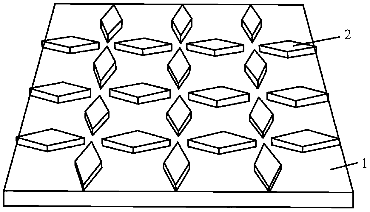
[0043] A broadband visible light absorber based on a semiconductor metasurface, comprising a metal reflective layer 1 and a dielectric layer 2 . The material of the metal reflection layer 1 is gold, and the thickness t is 100 nanometers. The material of the dielectric layer 2 is silicon, and the thickness h is 50 nanometers to 80 nanometers.

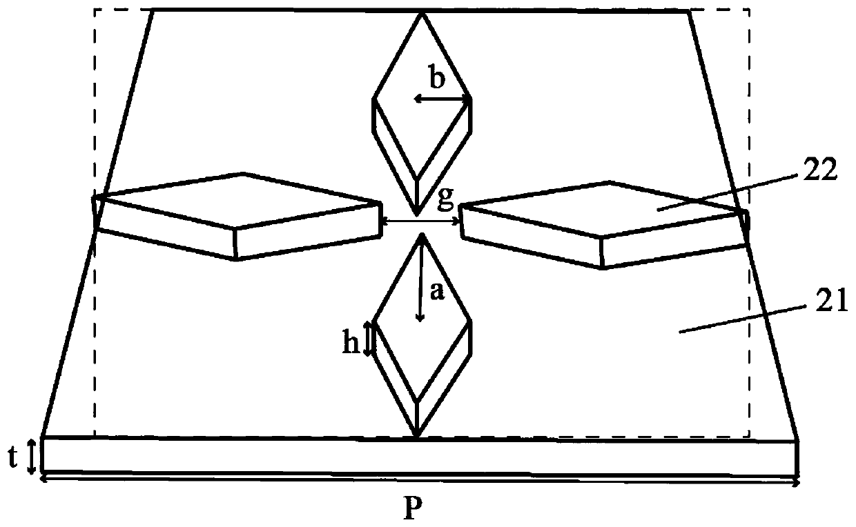
[0044] In order to prepare the above-mentioned absorber, first, the ion beam sputtering deposition method was used on the upper surface of the sapphire substrate to deposit a gold film with a thickness of 100 nanometers as the metal reflective layer 1, and the ion beam sputtering deposition method was used on the surface of the metal reflective layer 1. method, depositing a silicon film with a thickness of 70 nanometers as the dielectric layer 2, and then using the focused ion beam lithography method to etch the dielectric layer 2 to obtain the structure of the rhombus resonator 22, as shown in figure 1 shown.

[00...


PUM

PropertyMeasurementUnit
Thicknessaaaaaaaaaa
Thicknessaaaaaaaaaa
Semi-major axisaaaaaaaaaa

Abstract

The invention discloses a visible light broadband perfect absorber based on a semiconductor metasurface. The absorber is an optical metasurface structure and comprises a metal reflecting layer and a dielectric layer arranged on the reflecting layer; the dielectric layer is composed of periodic structure units and is a square; each structure unit is composed of four rhombus dielectric block resonators which are arranged in a crisscross shape; two adjacent structure units share on rhombus resonators. Compared with the existing absorber, the absorber has strong absorption effect on the incident light by utilizing the strong electromagnetic resonance mode of the dielectric resonators and a coupling resonance mode between the adjacent resonators, thereby realizing the broadband perfect absorption of the ultraviolet-visible-near infrared waveband.

Description

technical field [0001] The invention relates to the field of optics, and belongs to a visible light perfect absorber based on a semiconductor metasurface, in particular to a visible light broadband perfect absorber based on a semiconductor metasurface. Background technique [0002] Metamaterials with perfect light absorption properties are a new direction of development in the past decade. Perfect light absorbers are used in a wide range of fields, such as thermal radiation, photoelectric detection, biosensing, radar stealth, and solar thermal photovoltaics. At present, a variety of perfect absorbers have been designed. However, perfect absorbers can be divided into two types according to different absorption bands, one is narrowband absorber and the other is broadband absorber. Narrow-band absorbers can confine photons to specified wavelength bands. According to the number of absorption bands, they can be divided into single-band perfect absorbers and multi-band perfect ab...

Claims


Application Information

Patent Timeline
IPC IPC(8): G02B5/00G02B1/00
CPCG02B1/002G02B5/003
Inventor 刘海英李晨辉许家玮郑允宝
Owner SOUTH CHINA NORMAL UNIVERSITY
Why Eureka
Try Eureka