Photoelectric device packaging method and packaging structure

A technology of optoelectronic devices and packaging methods, which is applied in the direction of electric solid-state devices, electrical components, semiconductor devices, etc., can solve the problems of poor reliability of chips against cold and heat shocks, and solve the problem of solder pad cracking, high packaging efficiency and yield, and manufacturing process. simple effect

Pending Publication Date: 2019-09-03
58TH RES INST OF CETC
View PDF0 Cites 4 Cited by
  • Summary
  • Abstract
  • Description
  • Claims
  • Application Information

AI Technical Summary

Problems solved by technology

[0005] The purpose of the present invention is to provide a photoelectric device packaging method to solve the problem of poor thermal shock resistance and "ghosting" of chips packaged by the existing photoelectric device packaging method

Method used


Image

  • Photoelectric device packaging method and packaging structure
  • Photoelectric device packaging method and packaging structure
  • Photoelectric device packaging method and packaging structure

Examples


Embodiment 1

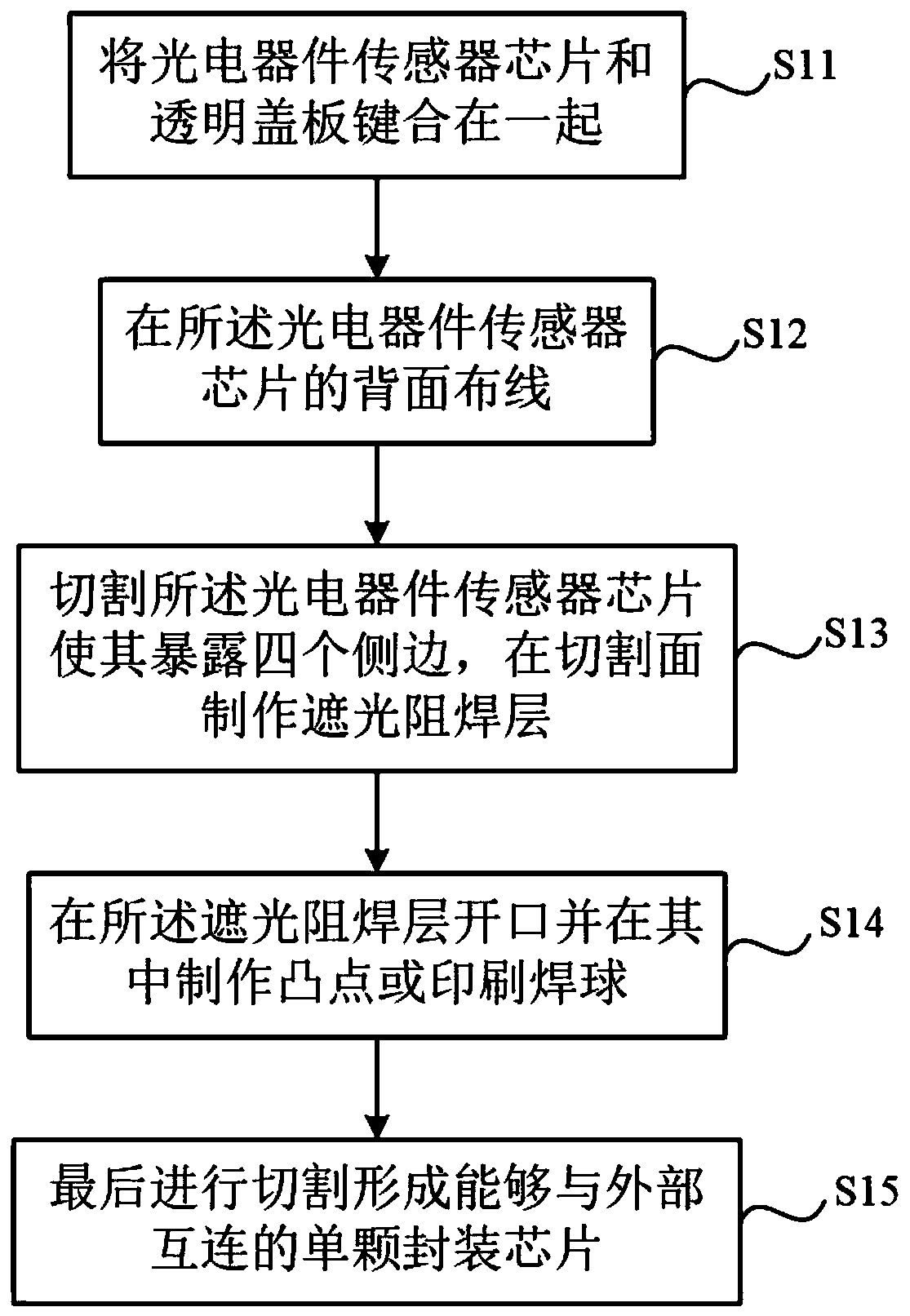
[0046] The invention provides a photoelectric device packaging method, the flow diagram of which is as follows figure 1 shown. The photoelectric device packaging method comprises the steps of:

[0047] Step S11, bonding the photoelectric device sensor chip and the transparent cover plate together;

[0048] Step S12, wiring on the back side of the photoelectric device sensor chip;

[0049] Step S13, cutting the photoelectric device sensor chip to expose four sides, and making a light-shielding solder resist layer on the cut surface;

[0050] Step S14, making an opening in the light-shielding solder resist layer and making bumps or printing solder balls therein;

[0051] Step S15 , finally cutting to form a single packaged chip that can be interconnected with the outside.

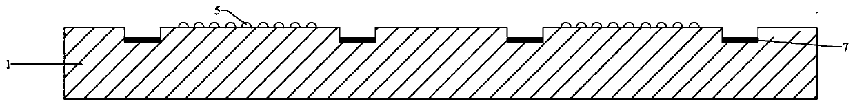
[0052] Firstly, the photoelectric device sensor chip is formed: a photoelectric device wafer is provided, and the photoelectric device wafer includes a silicon substrate 1 and a metal pad 7 and a photoele...

Embodiment 2

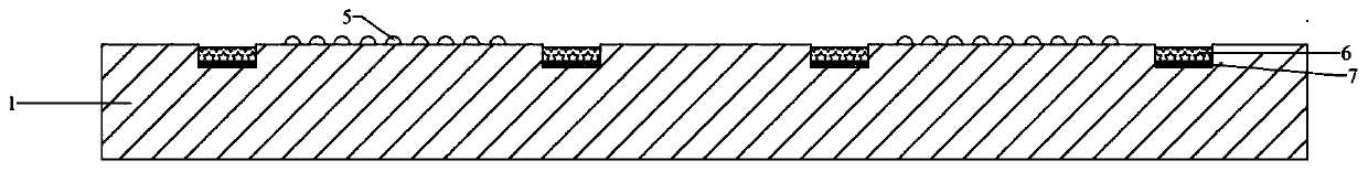
[0058] Embodiment 2 of the present invention also provides an optoelectronic device packaging structure prepared by the above optoelectronic device packaging method, the structure of which is as follows Figure 10 shown. The photoelectric device packaging structure includes a photoelectric device sensor chip, and the photoelectric device sensor chip includes a photoelectric device wafer, and the photoelectric device wafer includes a silicon substrate 1 and a metal pad 7 formed on the silicon substrate and a photoelectric sensor chip. Lens 5.

[0059] Specifically, the photoelectric device packaging structure also includes a transparent cover plate, which is bonded to the photoelectric device sensor chip; Layer 2; the thickness of the cofferdam and bonding layer 2 is 1 / 11~1 / 9 of the glass substrate 3, with a tolerance of ±3um, so as to ensure that the packaged photoelectric device has the best imaging quality. The photosensor microlens 5 is located in the cavity 4 jointly for...


PUM


Abstract

The invention discloses a photoelectric device packaging method and a packaging structure, and belongs to the technical field of integrated circuit packaging. The method comprises the steps of: bonding a sensor chip of a photoelectric device and a transparent cover plate together; performing wiring at the back of the sensor chip of the photoelectric device, cutting the sensor chip of the photoelectric device to expose four sides of the sensor chip, and manufacturing a shading and welding-resisting layer on the cutting surface; performing opening at the shading and welding-resisting layer, andmanufacturing salient points or printing solder balls in the shading and solder-resisting layer; and finally, performing cutting to form a single package chip mutually connected with the external portion.

Description

technical field [0001] The invention relates to the technical field of integrated circuit packaging, in particular to a photoelectric device packaging method and packaging structure. Background technique [0002] With the continuous improvement of the wafer tape-out process level of optoelectronic devices, the pixels of a single chip are also gradually increasing. For photoelectric device sensors, since the photosensitive components are distributed on the front side of the chip, the front side of the wafer needs to be bonded to the transparent substrate. On the one hand, it ensures that the light enters, and on the other hand, it also protects the photosensitive components from damage. Since the front side of the wafer is bonded to the transparent substrate, optoelectronic devices cannot be wired from the front side of the chip, so the photoelectric sensor chips using wafer-level packaging are wired on the back side of the chip through TSV through-hole technology. The packa...

Claims


Application Information

Patent Timeline
Patent Type & Authority Applications(China)
IPC IPC(8): H01L27/146
CPCH01L27/14618H01L27/14623H01L27/14632H01L27/14636H01L27/14687
Inventor 王成迁李杨朱家昌
Owner 58TH RES INST OF CETC
Why Eureka
Try Eureka