A printed circuit board and test fixture
A technology for printed circuit boards and backplanes, which is applied to printed circuits, printed circuit manufacturing, printed circuit components, etc., and can solve problems such as discontinuous impedance, increased test times, and low test efficiency
- Summary
- Abstract
- Description
- Claims
- Application Information
AI Technical Summary
Problems solved by technology
Method used
Image
Examples
Embodiment 1
[0019] The embodiments of the present application provide a printed circuit board, which will be described below.
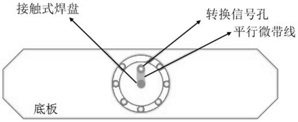
[0020] figure 2 A schematic top plan view of the contact pad of the printed circuit board in the embodiment of the present application is shown.
[0021] Examples of this application figure 2 Taking a single connection point as an example for illustration, as shown in the figure, the printed circuit board includes: a bottom plate, and one or more connection points, the bottom plate includes a plurality of layers, and the one or more connection points are located in the The outermost layer of the bottom plate, each connection point includes a contact pad and a conversion signal hole; the contact pad is connected with the conversion signal hole through a parallel microstrip line; the conversion signal hole is used to connect the other layers of the backplane.
[0022] During specific implementation, the printed circuit board in the embodiments of the present a...
Embodiment 2
[0061] Based on the same inventive concept, an embodiment of the present application provides a test fixture.
[0062] Figure 4 A schematic structural diagram of the test fixture in the embodiment of the present application is shown.
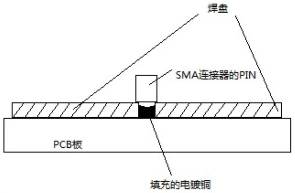
[0063] As shown in the figure, the test fixture includes: the printed circuit board as described in Embodiment 1, and an SMA connector, the PIN of the SMA connector is attached to the contact pad, and the SMA connector has The other end is connected with a transmission line, and the transmission line is used to connect the device under test.
[0064] During specific implementation, the device under test may be a device element such as a connector under test, an oscilloscope, and the like.
[0065] The SMA connector is free of soldering, and can be directly fixed and assembled with the printed circuit board by screws. The contact pad is located in the center of the SMA connector to ensure that the contact pad and the PIN of the SMA connector ...
Embodiment 3
[0078] The embodiments of the present application are described below with a specific example.
[0079] The bottom plate of the PCB is provided with 3 connection points A, B and C, and each connection point includes an SMA contact pad and a conversion signal hole; the SMA contact pad is connected to the conversion through parallel microstrip lines. The signal hole is connected; the conversion signal hole is used to connect different layers of the base plate.
[0080] The radius of the SMA contact pad is 0.2mm-0.4mm, the size of the conversion signal hole is 0.5mm, and the distance from the conversion signal hole to the center of the SMA contact pad is 0.5mm-2mm, The impedance of the conversion signal hole is 50 ohms. The line width of the parallel microstrip line can be calculated according to the impedance, and the impedance of the parallel microstrip line is 50 ohms.
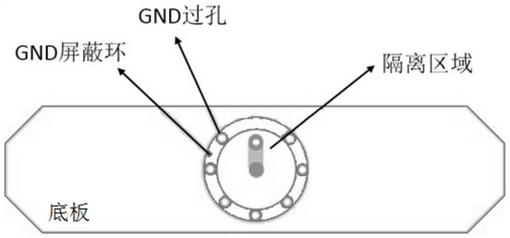
[0081] A GND shielding ring is arranged around the SMA contact pad and the conversion signal hole, the ra...
PUM
 Abstract
Description
Claims
Application Information


