Assembling method of miniaturized printed board

An assembly method and technology for printed boards, which are applied in the directions of printed circuits, printed circuit components, and electrical connection printed components, can solve the problems of difficult assembly and low integration of small printed boards, and achieve space saving, easy operation, and reduction in size. The effect of processing difficulty

Inactive Publication Date: 2019-09-10
SUZHOU R&D CENT OF NO 214 RES INST OF CHINA NORTH IND GRP
View PDF7 Cites 0 Cited by
  • Summary
  • Abstract
  • Description
  • Claims
  • Application Information

AI Technical Summary

Problems solved by technology

[0004] The technical problem to be solved by the present invention is to overcome the defects of the prior art, provide a miniaturized assembly method for printed boards, and solve the problems of low integration of small printed boards, difficulty in process layout, wiring, and assembly

Method used


Image

  • Assembling method of miniaturized printed board
  • Assembling method of miniaturized printed board
  • Assembling method of miniaturized printed board

Examples


Embodiment Construction

[0032] The present invention will be further described below in conjunction with the accompanying drawings. The following examples are only used to illustrate the technical solution of the present invention more clearly, but not to limit the protection scope of the present invention.

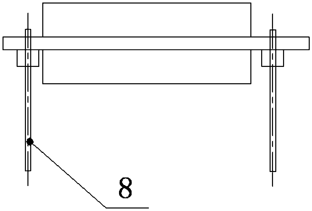
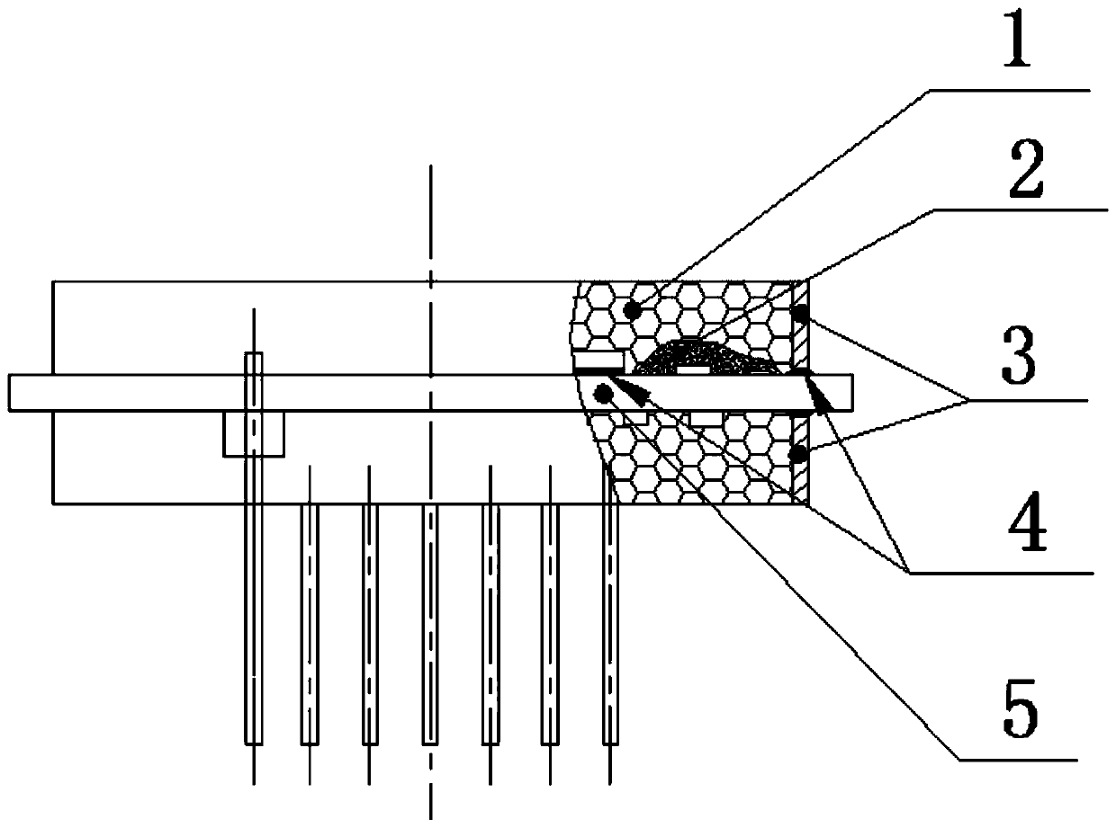
[0033] Such as figure 1 As shown in -4, what is adopted in the present invention is the miniaturized assembly technology of the printed board, which adopts the enclosing frame bonding (or welding) on ​​the PCB board 5, and then potting and encapsulating the technology for encapsulation. The PCB board 5 is a circular structure with three equally divided large mounting holes 9 on the edge for installing and fixing the PCB board 5 , the wiring area is irregular and the space is narrow. The outer lead pin 8 is drawn out by pin soldering. In the circuit on the PCB board 5, the resistors and power resistors that need active trimming are printed with a ceramic substrate thick film, which can be divid...


PUM


Abstract

The invention discloses an assembling method of a miniaturized printed board. A PCB adopts a circular structure, and a plurality of equal-size mounting holes are formed in the edge of the PCB; a surrounding frame is arranged on the periphery of a wiring area on the PCB; a bare chip and a gold wire bonding area arranged on the PCB are wrapped by binding glue, and then filling and sealing is carriedout on the area in the surrounding frame by using a pouring sealant, so as to realize non-airtight packaging. According to the method, the problems of low integration level, difficulty in process layout, wiring and assembling of the miniaturized printed board are solved.

Description

technical field [0001] The invention relates to a miniaturized assembly method of a printed board, which belongs to the technical field of printed board packaging. Background technique [0002] The known encapsulation technology of PCB printed board encapsulation is generally assembled by soldering separate components on the front of the printed board; the assembled pins are potted through the shell to realize the non-airtight encapsulation structure of the metal shell. [0003] The disadvantage of this packaging structure is that the device assembly density of a single PCB substrate is small, and the circuit size after assembly is large, and potting cannot be achieved for irregular circuit substrates. Contents of the invention [0004] The technical problem to be solved by the present invention is to overcome the defects of the prior art, provide a miniaturized printing board assembly method, and solve the problems of low integration of small printed boards, difficulty in...

Claims


Application Information

Patent Timeline
IPC IPC(8): H05K1/18H05K1/16H05K1/11H05K1/02H05K3/28H05K3/30H05K3/12
CPCH05K1/02H05K1/115H05K1/167H05K1/18H05K3/12H05K3/28H05K3/30
Inventor 聂月萍李军福杜松张君利
Owner SUZHOU R&D CENT OF NO 214 RES INST OF CHINA NORTH IND GRP
Why Eureka
Try Eureka