Electrolytic polishing method and device for semi-conductor materials

An electrolytic polishing and semiconductor technology, applied in the electrolytic process, electrolytic components, etc., can solve the problems of poor surface integrity of semiconductor materials, inability to improve the temperature, thickness, and parallelism of the electrolyte, and achieves the promotion of electrolytic polishing and novel structure. , the effect of reducing the temperature difference of electrolysis

Active Publication Date: 2019-09-20
江苏守航实业有限公司
View PDF50 Cites 2 Cited by
  • Summary
  • Abstract
  • Description
  • Claims
  • Application Information

AI Technical Summary

Problems solved by technology

[0003] Abrasive treatment such as grinding and lapping is a necessary way to produce semiconductor wafers. Polishing and planarization are very important for the production of microelectronic components. The traditional and most common polishing method is mechanical polishing. However, mechanical polishing is time-consuming and labor-intensive. It is easy to cause The error of thickness and parallelism will lead to the deterioration of the surface integrity of the semiconductor material, and it is easy to be broken and damaged. Therefore, electrolytic polishing can be used instead of mechanical polishing. Carry out special anodic treatment to obtain a smooth and bright surface finishing process to improve the processing accuracy of semiconductor materials. In the process of electrolytic polishing, generally the higher the temperature, the faster the polishing and leveling speed, and electrolytic polishing Stirring the electrolyte during polishing can promote the flow of the electrolyte and ensure the most suitable polishing conditions
[0004] Existing electropolishing devices for semiconductor materials have a simple structure. Generally, the anode is set as the workpiece to be polished, the anode and the cathode are connected through the electrolyte, and a direct current is used for electropolishing, but the temperature of the electrolyte cannot be increased, and It lacks the function of stirring the electrolyte, and the temperature and stirring have a certain influence on the speed of electropolishing, which makes the speed of electropolishing slow and the efficiency low. Therefore, we propose a method and device for electropolishing of semiconductor materials, which are used to solve the above problems

Method used


Image

  • Electrolytic polishing method and device for semi-conductor materials
  • Electrolytic polishing method and device for semi-conductor materials
  • Electrolytic polishing method and device for semi-conductor materials

Examples


Embodiment Construction

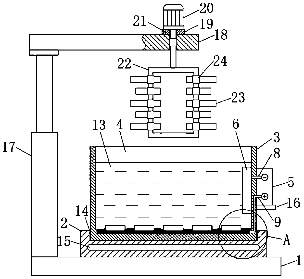
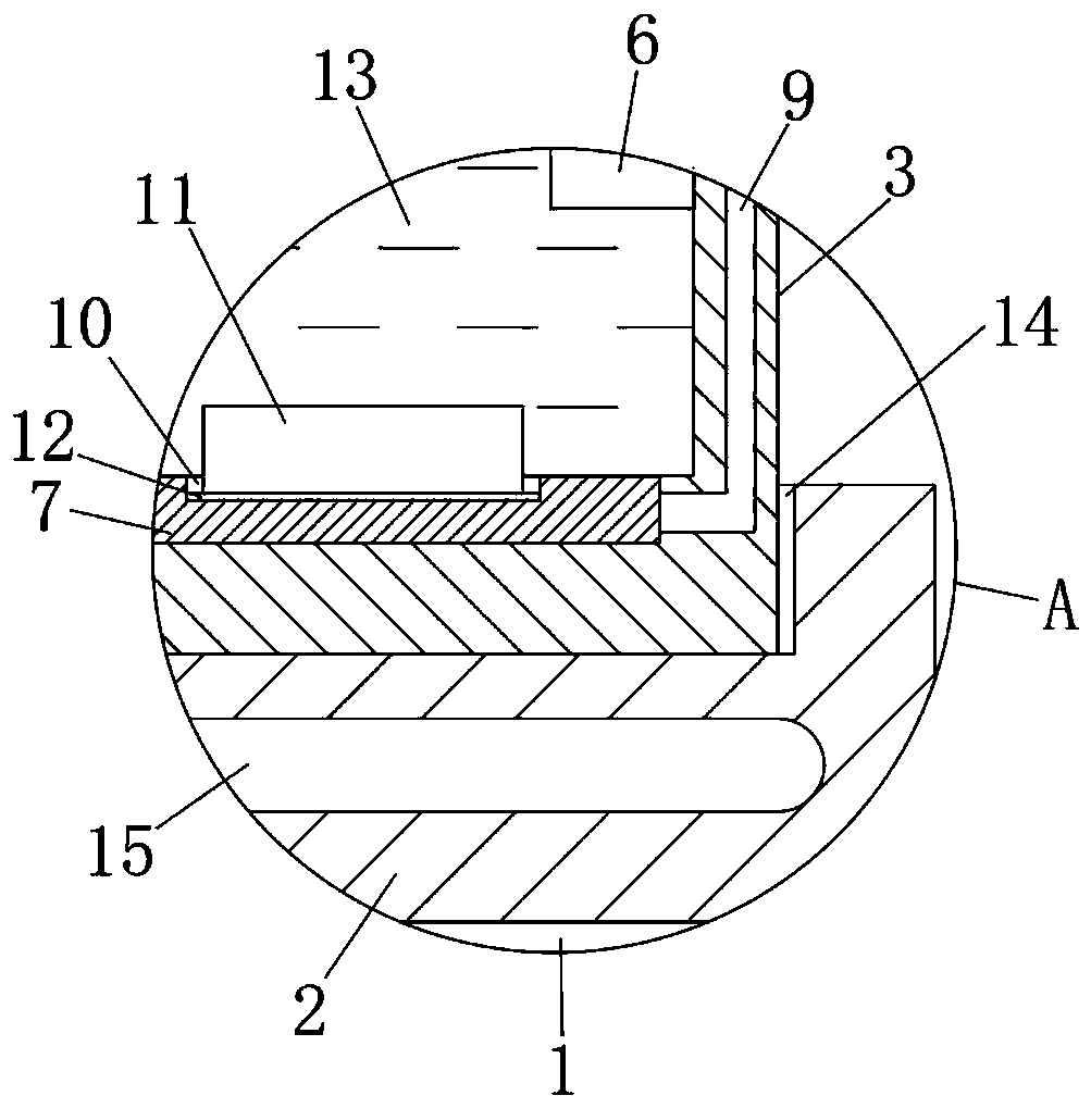
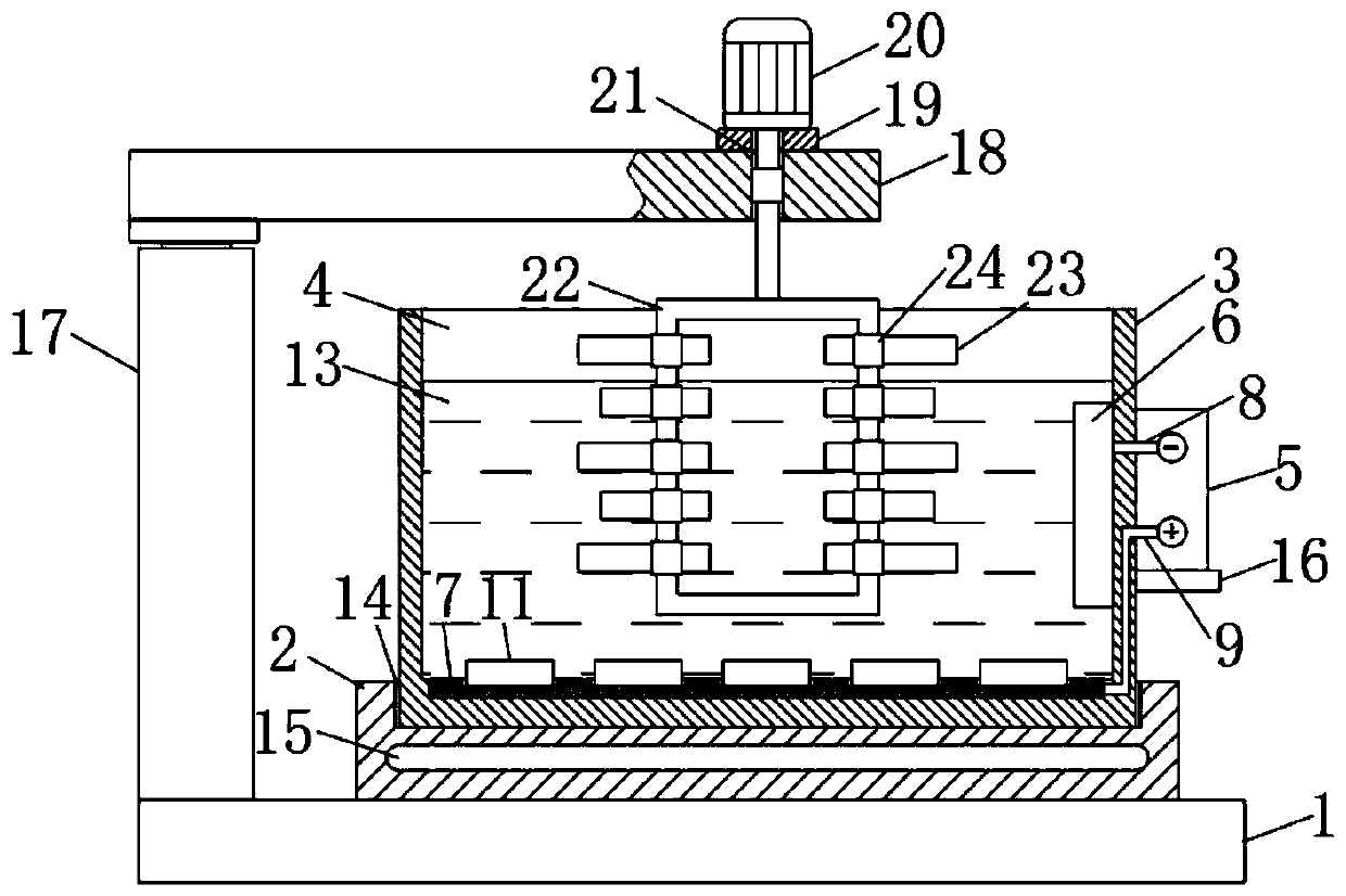
[0032] The technical solutions in the embodiments of the present invention will be clearly and completely described below with reference to the accompanying drawings in the embodiments of the present invention. Obviously, the described embodiments are only a part of the embodiments of the present invention, but not all of the embodiments.

[0033] In describing the present invention, it should be understood that the terms "upper", "lower", "front", "rear", "left", "right", "top", "bottom", "inner", " The orientation or positional relationship indicated by "outside", etc. is based on the orientation or positional relationship shown in the drawings, and is only for the convenience of describing the present invention and simplifying the description, rather than indicating or implying that the referred device or element must have a specific orientation, so as to Specific orientation configurations and operations, therefore, are not to be construed as limitations on the invention. ...


PUM

PropertyMeasurementUnit
electrical resistivityaaaaaaaaaa

Abstract

The invention discloses an electrolytic polishing device for semi-conductor materials. The electrolytic polishing device comprises a bottom plate. A device base is fixedly connected to the side wall of the upper end of the bottom plate. An electrolytic pool is arranged at the upper end of the device base. The invention further provides an electrolytic polishing method for the semi-conductor materials. The method comprises the following steps that 1, anodes of the multiple semi-conductor materials to be polished are prepared before electrolytic polishing, the surfaces of the anodes are subjected to primary manual polishing treatment, impurities remaining on the surfaces of the anodes are removed, and clear water is used for washing the surfaces of the anodes. The electrolytic polishing device is reasonable in structure and convenient to use; a heating device and a lifting stirring mechanism are arranged, by means of the heating device, the temperature of an electrolytic solution is increased, the speed of electrolytic polishing is increased beneficially, by means of the lifting stirring mechanism, flowing of the electrolytic solution can be prompted, ion diffusion of a polishing area and supplementing of a new electrolytic solution can be ensured, therefore electrolytic polishing of the anodes is prompted, and the efficiency of electrolytic polishing is improved.

Description

technical field [0001] The invention relates to the technical field of semiconductor material processing, in particular to an electrolytic polishing method and device for semiconductor materials. Background technique [0002] Materials in nature can be divided into three categories: conductors, semiconductors, and insulators according to their electrical conductivity. Among them, semiconductor materials are a class with semiconductor properties, that is, the electrical conductivity is between conductors and insulators, and the resistivity is about 1mΩ·cm~1GΩ· cm range, and can be used to make electronic materials for semiconductor devices and integrated circuits. [0003] Abrasive treatment such as grinding and grinding is a necessary way to produce semiconductor wafers. Polishing and planarization are very important for the production of microelectronic components. The most common traditional polishing method is mechanical polishing. However, mechanical polishing is not onl...

Claims


Application Information

Patent Timeline
Patent Type & Authority Applications(China)
IPC IPC(8): C25F3/30C25F7/00
CPCC25F3/30C25F7/00
Inventor 魏守冲
Owner 江苏守航实业有限公司
Why Eureka
Try Eureka