Dimming device
A dimming device and dimming element technology, which is applied in optics, output power conversion devices, nonlinear optics, etc., can solve the problems of low power conversion efficiency and large power consumption of dimming devices, so as to reduce power consumption Effect
- Summary
- Abstract
- Description
- Claims
- Application Information
AI Technical Summary
Problems solved by technology
Method used
Image

Examples
no. 1 Embodiment approach
[0024] [1] Structure of the dimming device 10
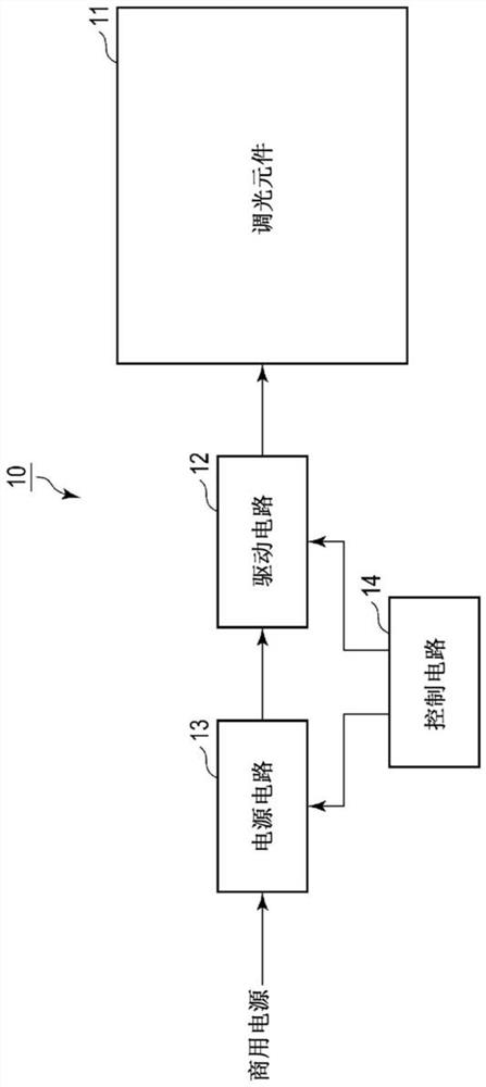
[0025] figure 1 This is a block diagram of the dimming device 10 according to the first embodiment of the present invention. The dimming device 10 includes a dimming element 11 , a driving circuit 12 , a power supply circuit 13 , and a control circuit 14 .
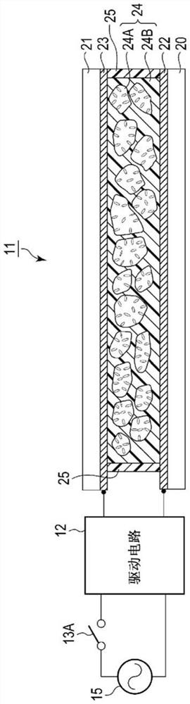
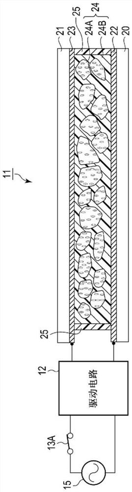
[0026] The dimming element 11 is an element capable of controlling the transmittance of light. The light control element 11 is formed of, for example, a light control film. The light control film is a functional film that can instantaneously switch between transparent and opaque (white turbidity) by turning on / off the power supply. An example of the structure of the light control element 11 will be described later.
[0027] The driving circuit 12 applies a voltage to the dimming element 11 to drive the dimming element 11 . The circuit configuration of the drive circuit 12 will be described later.
[0028] The power supply circuit 13 receives AC power from the outside. ...
no. 2 Embodiment approach
[0109] In the second embodiment, the alternating voltage is intermittently removed locally or periodically.
[0110] Figure 12 It is a timing chart explaining the operation of the drive circuit 12 according to the second embodiment of the present invention. The operation until time t0 to t6 is the same as that of the first embodiment Figure 7 same.
[0111] like Figure 5 As shown, the intermittent rejection circuit 40 receives the output of the comparator CP3 for zero-cross detection. The cull circuit 40 sends the cull pattern to the timing generation circuit 39 .
[0112] The intermittent rejection circuit 40 outputs a low level as the intermittent rejection mode from time t0 to t6. For example, when the intermittent culling mode is at the low level, the timing generation circuit 39 generates a signal for causing the transistors T1 and T2 to switch on and off.
[0113] At time t6, the comparator CP3 for zero crossing outputs a high level. Receiving the output of the...
Embodiment
[0120] In each of the above-described embodiments, the liquid crystal element (light control element) using PDLC or PNLC is exemplified, but the present invention is not limited to this. The liquid crystal element may have a structure in which polarizing plates and alignment films are arranged on both sides of the liquid crystal layer, and a TN (Twisted Nematic) method, a VA (Vertical Alignment) method, or an IPS (In-Plane Switching) method can be used. Moreover, as a light control element, besides a liquid crystal element, various electro-optical elements whose refractive index is changed by a voltage can be used.
[0121] In addition to MOS transistors or bipolar transistors, the switching elements T1 and T2 shown in the above-described embodiments may be SiC-MOSFETs using silicon carbide (SiC) as the semiconductor layer or gallium nitride (GaN) as the semiconductor layer. ) of GaN-MOSFET etc.
[0122] In addition to diodes, the rectifier elements D3 and D4 shown in the abo...
PUM
 Abstract
Description
Claims
Application Information