Supercharge Your Innovation With Domain-Expert AI Agents!

3D NAND memory and method of forming the same

A 3D NAND and memory technology, applied in the direction of semiconductor devices, electrical solid devices, electrical components, etc., can solve the problems of easy tilting of the gate spacer, short circuit between the gate spacer and the channel via hole, etc., and achieve easy stress difference Effect

Active Publication Date: 2020-04-10
YANGTZE MEMORY TECH CO LTD
View PDF4 Cites 0 Cited by
  • Summary
  • Abstract
  • Description
  • Claims
  • Application Information

AI Technical Summary

Problems solved by technology

[0004] Existing memories generally include several memory blocks (Blocks), and the memory blocks are generally separated by Gate Line Slits (GLS) vertically penetrating the stacked structure. However, existing 3D NAND memories During the process, the gate spacer in some areas is easy to tilt, resulting in a short circuit between the gate spacer and the channel via hole

Method used


Image

  • 3D NAND memory and method of forming the same
  • 3D NAND memory and method of forming the same
  • 3D NAND memory and method of forming the same

Examples


no. 1 example 3D

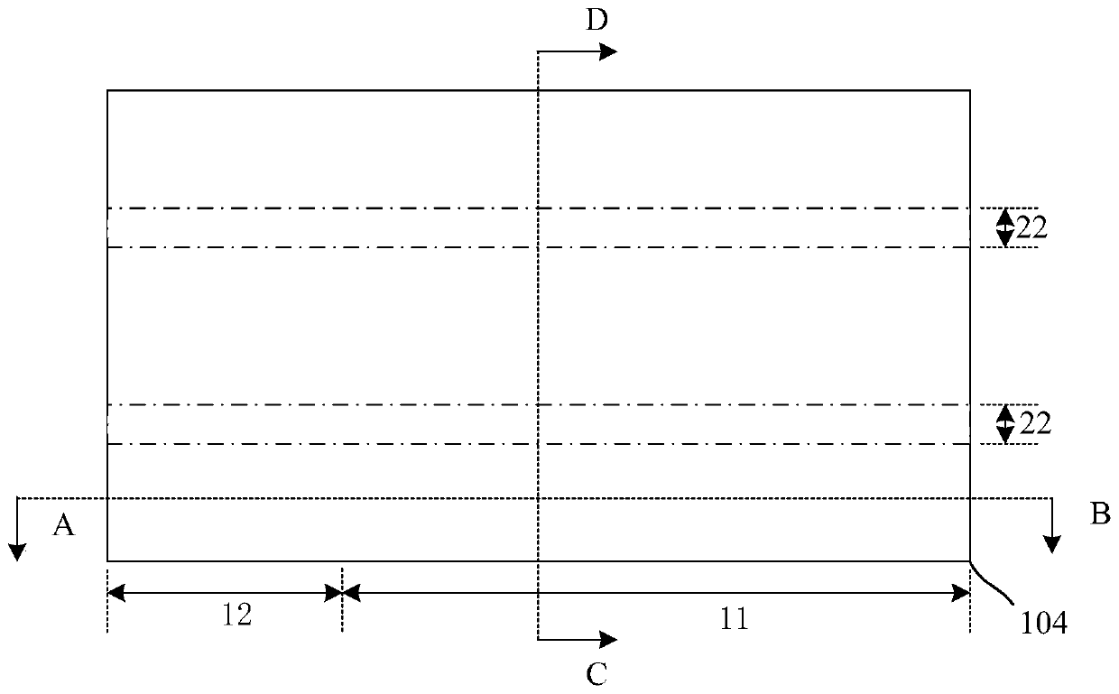
[0053] Figure 1-Figure 14 It is a structural schematic diagram of the 3D NAND formation process according to the first embodiment of the present invention.

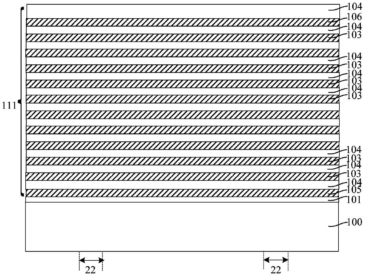
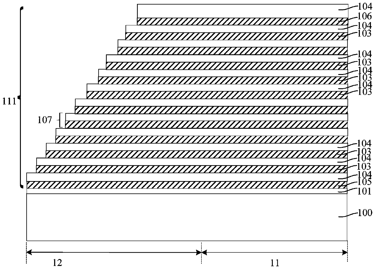
[0054] refer to figure 1 and figure 2 , figure 2 for figure 1 A schematic diagram of a cross-sectional structure along a cutting line CD provides a semiconductor substrate 100 on which a stacked structure 111 in which sacrificial layers 103 and isolation layers 104 are alternately stacked is formed.

[0055] The material of the semiconductor substrate 100 can be single crystal silicon (Si), single crystal germanium (Ge), or silicon germanium (GeSi), silicon carbide (SiC); it can also be silicon on insulator (SOI), germanium on insulator (GOI); or other materials, such as III-V group compounds such as gallium arsenide. In this embodiment, the material of the semiconductor substrate 100 is single crystal silicon (Si).

[0056] The stacked structure 111 includes several alternately stacked sacrificial layers 103 an...


PUM


Abstract

A 3D NAND memory and its forming method, the forming method is by making the density of the dummy channel vias in the dummy channel via adjustment area greater than the dummy channel vias in the step area outside the dummy channel via adjustment area Density, the density of the dummy channel structures in the dummy channel vias in the corresponding dummy channel via adjustment area is greater than that in the dummy channel vias in the step area outside the dummy channel via adjustment area , the difference between the density of the dummy channel structures in the dummy channel vias in the dummy channel via adjustment region and the density of the memory structures in the channel vias in the channel via adjustment region is reduced, so that The difference in stress of the thin film in the stacked structure on both sides of or near the junction of the step region and the core region will be reduced, so when the stack structure at the junction of the step region and the core region is etched to form a gate spacer, the junction will be The sidewalls of the gate spacer are not inclined or the inclination is greatly reduced, thereby preventing the gate spacer from being short-circuited with the channel via hole.

Description

technical field [0001] The invention relates to the field of semiconductor manufacturing, in particular to a method for reducing 3D NAND memory. Background technique [0002] NAND flash memory is a non-volatile storage product with low power consumption, light weight and good performance, and has been widely used in electronic products. At present, the planar NAND flash memory is close to the limit of practical expansion. In order to further increase the storage capacity and reduce the storage cost per bit, a 3D NAND memory with a 3D structure is proposed. [0003] The formation process of the existing 3D NAND memory generally includes: forming a stacked structure in which isolation layers and sacrificial layers are alternately stacked on the substrate; etching the stacked structure, forming channel vias in the stacked structure, and forming channel vias Finally, etch the substrate at the bottom of the channel via hole to form a groove in the substrate; in the groove at the...

Claims


Application Information

Patent Timeline
Patent Type & Authority Patents(China)
IPC IPC(8): H01L27/11551H01L27/11524H01L27/1157H01L27/11578H10B41/20H10B41/35H10B43/20H10B43/35
CPCH10B41/35H10B41/20H10B43/35H10B43/20
Inventor 王香凝耿静静王攀张慧刘新鑫吴佳佳肖梦
Owner YANGTZE MEMORY TECH CO LTD
Features
  • R&D
  • Intellectual Property
  • Life Sciences
  • Materials
  • Tech Scout
  • Unparalleled Data Quality
  • Higher Quality Content
  • 60% Fewer Hallucinations
Learn More