3D NAND memory and forming method thereof
一种3DNAND、存储器的技术,应用在半导体器件、电固体器件、气候可持续性等方向,能够解决栅极隔槽与沟道通孔短路、栅极隔槽易倾斜等问题
- Summary
- Abstract
- Description
- Claims
- Application Information
AI Technical Summary
Problems solved by technology
Method used
Image

Examples
no. 1 example 3D
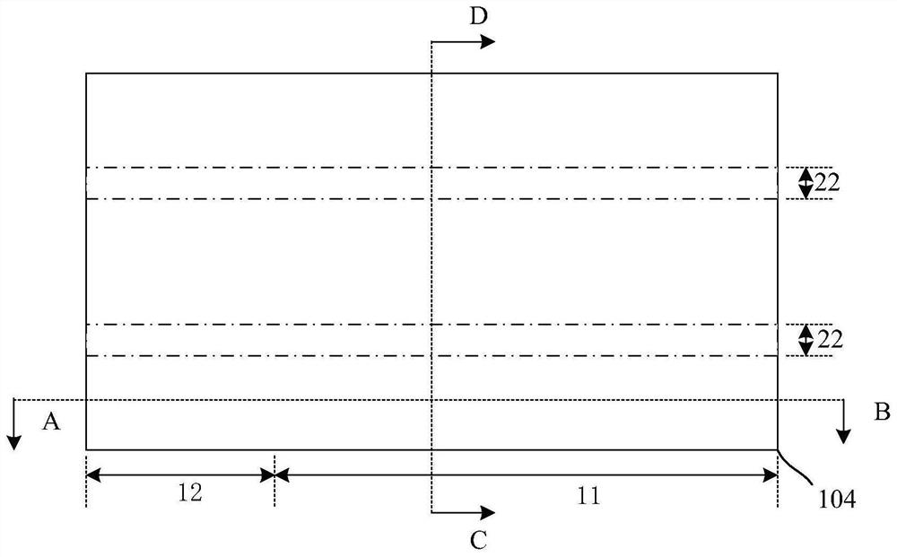
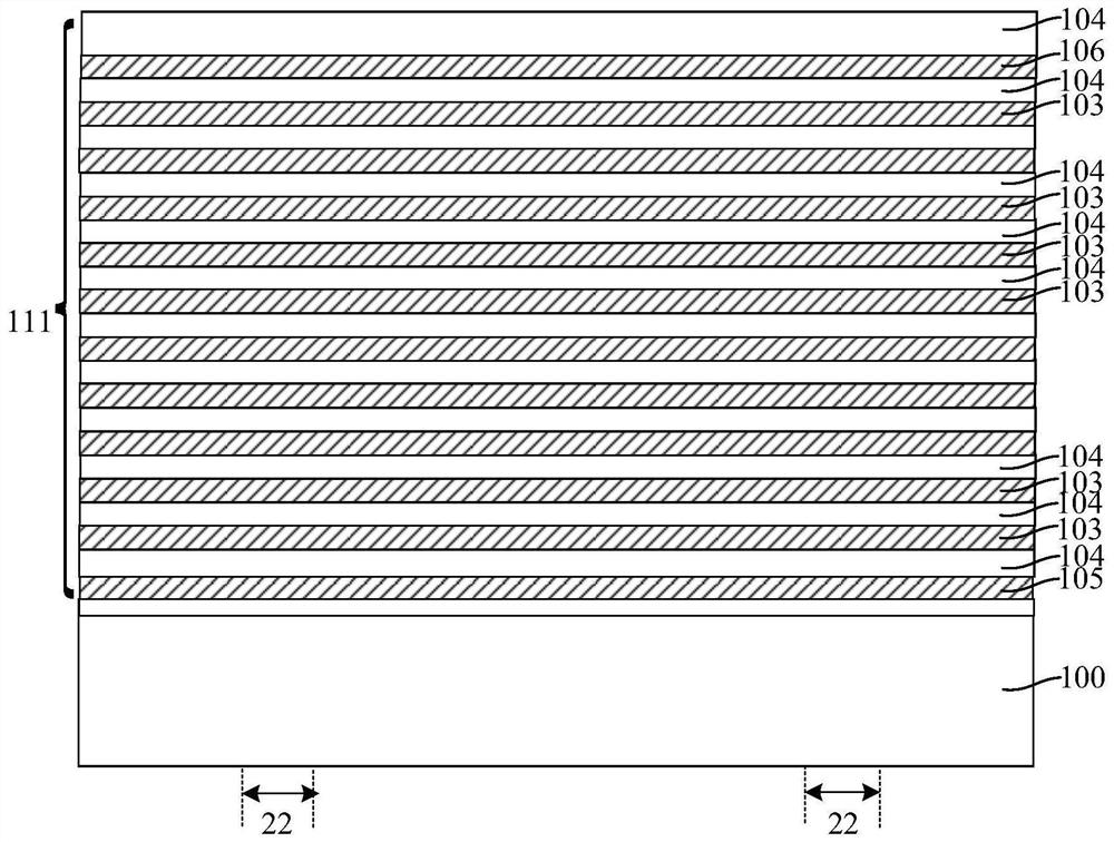
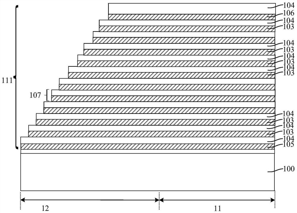
[0073] Figure 1-Figure 14 It is a schematic structural diagram of a 3D NAND formation process according to the first embodiment of the present invention.
[0074] refer to figure 1 and figure 2 , figure 2 for figure 1 A schematic cross-sectional structure diagram along the cutting line CD direction provides a semiconductor substrate 100 on which a stack structure 111 in which sacrificial layers 103 and isolation layers 104 are alternately stacked is formed.
[0075] The material of the semiconductor substrate 100 can be single crystal silicon (Si), single crystal germanium (Ge), or silicon germanium (GeSi), silicon carbide (SiC); it can also be silicon on insulator (SOI), germanium on insulator (GOI); or other materials, such as Group III-V compounds such as gallium arsenide. In this embodiment, the material of the semiconductor substrate 100 is single crystal silicon (Si).
[0076] The stacked structure 111 includes several alternately stacked sacrificial layers 103...
PUM
 Abstract
Description
Claims
Application Information
 - R&D
- Intellectual Property
- Life Sciences
- Materials
- Tech Scout
- Unparalleled Data Quality
- Higher Quality Content
- 60% Fewer Hallucinations
Browse by: Latest US Patents, China's latest patents, Technical Efficacy Thesaurus, Application Domain, Technology Topic, Popular Technical Reports.
© 2025 PatSnap. All rights reserved.Legal|Privacy policy|Modern Slavery Act Transparency Statement|Sitemap|About US| Contact US: help@patsnap.com