

Test structure for monitoring backside-illumination electronegativity intensity and process integration method
A test structure, back-illuminated technology, used in semiconductor/solid-state device testing/measurement, circuits, electrical components, etc., can solve the problems of prolonged development cycle, lag, waste of silicon wafers, etc., and achieve low process cost and low test cost. , Test the effect of convenience
- Summary
- Abstract
- Description
- Claims
- Application Information
AI Technical Summary
Problems solved by technology
Method used
Image

Examples
Embodiment Construction
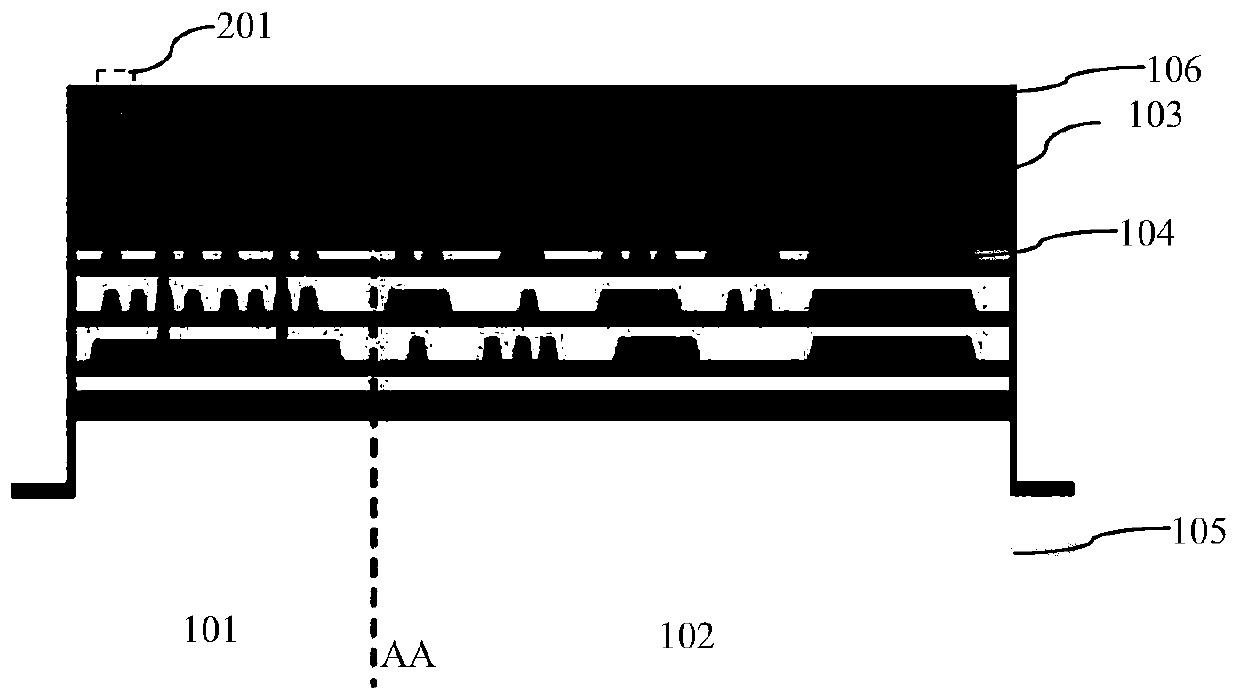
[0059] First of all, the structure of the existing back-illuminated image sensor will be described in conjunction with the accompanying drawings:
[0060] like Figure 1A As shown, it is a schematic structural diagram of an existing back-illuminated image sensor; the existing back-illuminated image sensor includes a pixel area 101 and a peripheral area 102, which are respectively located on the left and right sides of the dotted line AA; on a semiconductor substrate such as a silicon substrate 103 A device structure is formed on it, and the semiconductor substrate 103 is also called a device sheet; the device structure in the pixel region 101 includes a photodiode, that is, a photodiode. Usually, the semiconductor substrate 103 is P-type doped, and the photodiode is formed on a P-type semiconductor The substrate 103 is composed of an N-type photosensitive doped region formed in the P-type semiconductor substrate 103 . CMOS devices are formed in the peripheral region 102 .
[...
PUM
 Abstract
Description
Claims
Application Information