

Array substrate, display panel and display apparatus
A technology of array substrate and substrate substrate, which can be used in instruments, organic semiconductor devices, digital data processing components, etc., and can solve problems such as the influence of electroluminescent devices
- Summary
- Abstract
- Description
- Claims
- Application Information
AI Technical Summary
Problems solved by technology
Method used
Image

Examples
Embodiment Construction
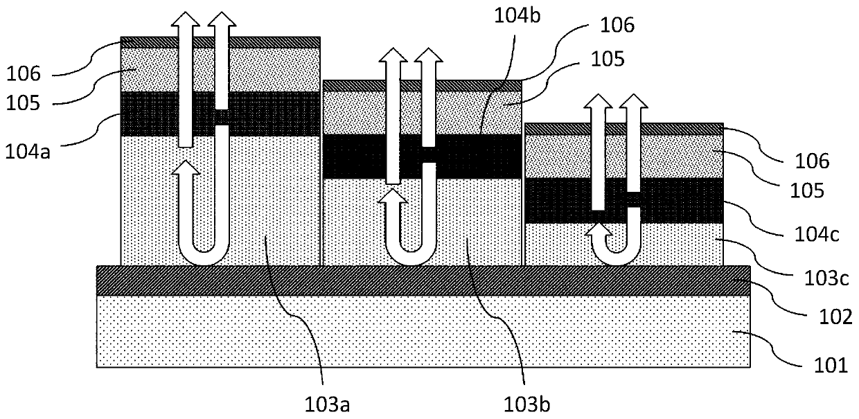
[0048] Array substrates in the related art, such as figure 1 As shown, among them, figure 1It is a top-emitting array substrate, that is, the light-emitting surface of the array substrate is located on the side away from the base substrate 101, and the array substrate includes: a base substrate 101, and a metal reflective electrode 102 located on the base substrate 101 for electrically The light emitted by the luminescent device is reflected, thereby enhancing the display brightness of the display panel; it also includes electroluminescent devices arranged in an array on the side of the metal reflective electrode 102 away from the substrate substrate, and each electroluminescent device includes sequentially stacked metal Reflective electrode 102, hole transport layer 103 (a, b or c), light emitting layer 104 (a, b or c), electron transport layer 105 (a, b or c) and upper electrode 106, wherein figure 1 The array substrate shown multiplexes the metal reflective electrode 102 a...
PUM
 Abstract
Description
Claims
Application Information