
An X-band metamaterial wave-absorbing sensor

A sensor and metamaterial technology, which is applied in the direction of material analysis using microwave means, material analysis through electromagnetic means, and material capacitance, can solve the problems of large size and low sensitivity of metamaterial wave-absorbing sensors, and achieve reduced size and improved Sensitivity, effect of increasing volume ratio

Active Publication Date: 2022-06-17
SOUTHWEST UNIV
View PDF4 Cites 0 Cited by
  • Summary
  • Abstract
  • Description
  • Claims
  • Application Information

AI Technical Summary

Problems solved by technology

[0004] In order to solve the problem of large size and low sensitivity of the metamaterial wave-absorbing sensor, the present invention aims to provide an X-band single absorption peak high-sensitivity wave-absorbing sensor, which can be excited around the resonator by optimizing and adjusting the structure design and its parameters. Strong electrical resonance mode, achieving more than 99% absorbing performance

Method used


Image

  • An X-band metamaterial wave-absorbing sensor
  • An X-band metamaterial wave-absorbing sensor
  • An X-band metamaterial wave-absorbing sensor

Examples


Embodiment Construction

[0027] In order to clearly illustrate the present invention, the present invention will be further described below with reference to the accompanying drawings.

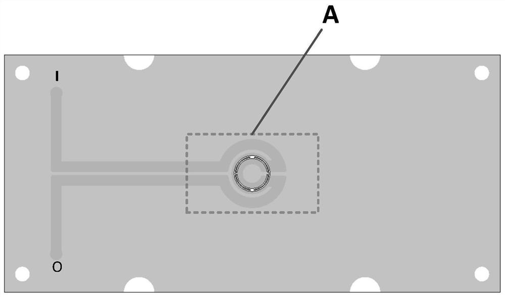
[0028] The wave absorbing sensor involved in the present invention is based on a single resonant unit A to achieve the wave absorbing performance described in the present invention, that is, the metamaterial wave absorbing sensor only includes one wave absorbing resonance unit, such as figure 1 As shown by the rectangular box, electromagnetic waves will be directed into the unit. The metal bottom plate, bottom substrate, microfluidic layer and top substrate in the resonance unit are properly extended in the x and y directions to achieve the purpose of adapting to the size of the test waveguide and form a complete metamaterial wave absorbing sensor. The four through holes at the top corners of the sensor are used to align each layer of the board, and the four upper and lower semicircular through holes are used to assem...


PUM

PropertyMeasurementUnit
angleaaaaaaaaaa
angleaaaaaaaaaa
thicknessaaaaaaaaaa

Abstract

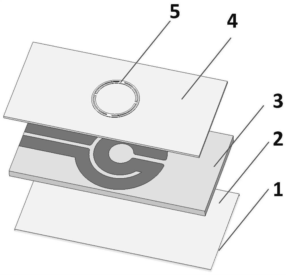
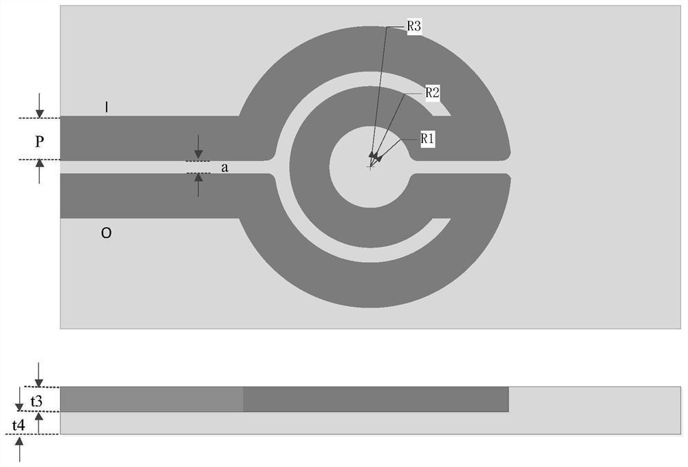
The invention relates to an X-band metamaterial wave-absorbing sensor, which is divided into three layers from bottom to top. The first layer is a metal bottom plate and a bottom substrate, the second layer is a microfluidic layer, and the third layer is a top substrate and a resonator. , the three-layer structure is bonded into one to form a wave-absorbing resonance unit. The resonator is formed on the top substrate and has an inner and outer double annular structure. The microfluidic channel layer is etched with a double-ring groove in the upper part to form microfluidic channels. The microfluidic channels are distributed on the side facing the resonator. Strong electric field resonance region. After the measured liquid is injected into the sensor, the dielectric constant of the microfluidic area can be changed, causing a shift in the absorption frequency point. The degree of shift can be used as a characteristic parameter of different measured liquids. When the relative dielectric constant of the measured liquid changes from 1 to 4.6, the sensor can achieve an average offset of 339MHz / unit dielectric constant, and the absorption rate remains above 95%.

Description

Technical field [0001] The invention relates to a metamaterial wave-absorbing sensor and belongs to the field of microwave sensing and detection. Background technique [0002] Metamaterial is a kind of artificial composite material with strange electromagnetic properties. It can exhibit many properties that are difficult to exist in nature, such as negative magnetic permeability, negative refractive index, etc. Metamaterials are generally planar structures that are easy to manufacture and integrate. Since artificial design has clear goals, continuous optimization of structures and exploration of new structures, metamaterials can be made into ultra-thin finished products for easy practical application. [0003] In 2010, Na Liu et al. successfully designed the first metamaterial wave-absorbing sensor. Simulations showed that the sensor could sense and detect different glucose solutions. Because of its advantages as a metamaterial, it quickly attracted the attention of many sc...

Claims


Application Information

Patent Timeline
Patent Type & Authority Patents(China)
IPC IPC(8): G01N22/00G01N27/22
CPCG01N22/00G01N27/221
Inventor 黄杰琚宗德徐国庆魏治华李俊杉倪星生刘旭阳
Owner SOUTHWEST UNIV
Learn More